
SEMICONDUCTOR REVIEW THANK YOU FOR SUBSCRIBING
× 
Semi Conductor Review Weekly Brief
Be first to read the latest tech news, Industry Leader's Insights, and CIO interviews of medium and large enterprises exclusively from Semi Conductor Review
Semiconductor Review: Specials Magazine

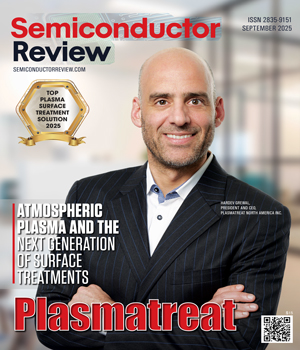
The semiconductor industry relies on vacuum chambers for plasma surface treatment because the method is proven, effective, and well established. However, the model comes at a cost: high capital investment, complex infrastructure, limited throughput, and minimal flexibility for inline production. As devices shrink and become more sensitive, these trade-offs intensify. Technical inertia is not the only barrier. Many engineers believe plasma can only exist in a vacuum, while atmospheric pressure plasma (APP) use damages delicate surfaces or produces harmful byproducts such as ozone. These perceptions have slowed the adoption of alternatives, even as the need for faster, cleaner, and safer processes grows urgent. The future of surface treatment requires breaking these assumptions, and Plasmatreat is leading the shift with its atmospheric plasma solutions that operate in open air, eliminate costly vacuum infrastructure, and increase throughput. Its Openair-Plasma® technology provides manufacturers with inline processing capabilities ideally suited for highly sensitive electronic components, efficiently replacing vacuum chambers and wet chemical cleaning in chip packaging. Beyond its technical advantages, the technology also introduces an environmental benefit. By replacing chemicals and reducing energy demands, it makes production cleaner, safer, and more sustainable, setting a new benchmark for the industry. “Our technology has a small carbon footprint, uses a zero-potential plasma jet, and produces no harmful byproducts such as ozone. From wafer-level treatments to AI-driven packaging, power modules, and final assemblies, we enable innovation across the entire electronics spectrum rather than a narrow niche,” says Hardev Grewal, president and CEO.
Top Semiconductor Incubators And Accelerators Solution 2025
Turning a chip idea into a successful company demands resilience, significant capital, rare engineering expertise, and years of focused development. Even Nvidia’s CEO, Jensen Huang has admitted he would not start a chip company again, given the scale of the challenge. The semiconductor world is tough to break into, but for bold founders, Silicon Catalyst, the only incubator and accelerator in the world focused exclusively on semiconductors, offers a purpose-built ecosystem that transforms complexity into opportunity and helps deep tech startups succeed. The company was built around a single question—how can semiconductor innovation become possible again? What started as a response to a gap in the market has evolved into a globally reputed accelerator for chip development and commercialization. “We’re doing God’s work in the semiconductor industry, helping startups” said Pete Rodriguez, CEO at Silicon Catalyst. Breaking Barriers in a High-Stakes Industry Many semiconductor startups struggle to access the most basic building blocks for development, including expensive EDA software, access to foundries, and trusted industry expertise. Silicon Catalyst tackles these issues with a multi-layered support model. Startups receive access to In-Kind Partner (IKP) goods and services from over 70 partners, including major players like Synopsys, Arm, TSMC, and Global Foundries. Portfolio Companies also have the opportunity to showcase their innovations to the numerous Silicon Catalyst Strategic Partners, including Arm, ST, NXP, DuPont, EMD Electronics, SMD Semiconductor, and Dexerials. Equally important is the human capital the incubator brings. Nearly 400 experienced advisors, many of them retired executives or technical leads, offer strategic and technical guidance. Each startup is paired with a senior partner who typically works with the company for at least two years. The guidance provided is hands-on, deeply technical, and aligned with each startup’s specific journey. A key value for the companies admitted to the 24-month Silicon Catalyst program is the development of an effective go-to-market strategy, for both new customer prospecting and investor outreach.

Top Counterfeit Electronics Mitigation Solution 2025

Critical systems, such as radars, communications networks, medical devices, and energy infrastructure, are designed to operate for decades; yet, the semiconductor components that power them are often produced for only a few years. SMT Corp keeps these systems running by sourcing and validating obsolete components. The company also helps shape and advance counterfeit detection methodologies, strengthening assurance across the supply chain. Through comprehensive inspection, testing, and verification, the company supplies its clients with fully authenticated, quality-assured components that meet stringent regulatory standards. With about 25 years of experience, the company is highly accredited and trusted, a reputation that sets it apart in the industry. In doing so, it bridges the divide between fast- changing semiconductor technology and the extended operational life of essential systems, helping preserve their safety, reliability, and performance. Regulatory requirements, such as those from the US Department of Defense, demand complete traceability and stringent testing for any parts sourced from beyond original manufacturers or authorized suppliers. SMT provides end-to-end inspection and test solutions that meet these demands while building confidence through industry-leading expertise and accreditation. Defining the Next Generation of Detection Semiconductor components often have short production lifespans with microcontrollers and FPGAs, for example, typically available form authorized sources for only four to seven years. Many critical systems in defense, aerospace, medical, and energy sectors remain in service for decades, creating a persistent gap between component availability and a system’s operational life. “Many of our customers operate systems whose lifespan far exceeds that of the parts they require,” explains Michael Schwarm, chief growth officer. “They depend on components that are no longer manufactured or readily available.” When customers request obsolete parts, authentic components are often difficult to source. Those found on the gray market frequently lack traceability, increasing the risk of counterfeit or degraded parts entering critical systems. To counter this, SMT employs rigorous inspection and testing to verify quality and authenticity before delivery.
CXO INSIGHTS

Accelerate the Semiconductor Workflow with a Standardized Measurement Framework
Mike Watts, Head of Industry Marketing, Semiconductor and Electronics, NI (National Instruments)

Selective Conformal Coating in Electronics Manufacturing
Jon Urquhart, Director - Global Applications Engineering, PVA

Test and Quality, Creston's Approach to Customer Loyalty
Ivan Farias, Senior Director, Production Operations, Crestron Electronics

Managing the security risks of IOT devices
Steve Hanna, Distinguished Engineer, Infineon Technologies

Is Design Reuse a Myth For Analog Circuits?
Eric Young, Senior Analog IC Design Manager, Monolithic Power Systems [NASDAQ: MPWR]

The Devolution & Revolution of Factory Operations
Christopher Downing, Senior Director of Operations/Manufacturing, MKS Instruments

Cots VS. Custom
Al Doyle, Corporate Vice President and CIO, Vicor Corporation


IN FOCUS
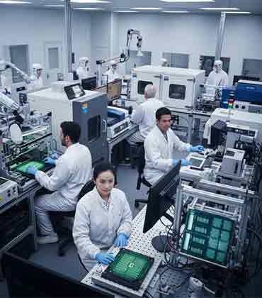
Semiconductor Incubation Platforms Shaping Tomorrow's Tech Landscape
Semiconductor incubators and accelerators support startups with infrastructure, funding, and expertise, addressing key challenges and fostering collaboration.
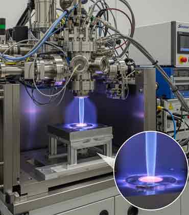
Digital Plasma Systems Supporting Next-Generation Product Performance
Plasma surface treatments enhance materials and are increasingly used in electronics, healthcare, automotive, and aerospace industries.
EDITORIAL
Adapting to Change in a Transforming Semiconductor Landscape
As the semiconductor industry navigates rapid technological change and rising market demands, it stands at a critical inflection point. Companies are under pressure to scale production, adopt next-generation technologies and secure increasingly complex global supply chains. The challenges are substantial, but with these challenges come significant opportunities to redefine the future of semiconductor manufacturing.
One area of transformative potential lies in Plasma Surface Treatment Solutions. As semiconductor production demands ever-higher precision, surface treatment technologies have become integral to improving the performance and longevity of components. Companies like Plasmatreat are leading the way with their advanced plasma technologies, which enhance the functionality of semiconductor materials through more advanced, efficient and sustainable processes. By providing superior bonding, cleaning and coating capabilities, plasma treatment is allowing manufacturers to meet the exacting standards of today's high-performance electronics.
At the same time, the industry is seeing the rise of semiconductor incubators and accelerators, which play a critical role in fostering the next generation of innovation. These initiatives are essential for nurturing startups and entrepreneurs who are developing breakthrough technologies. By providing access to funding, mentorship and state-of-the-art facilities, incubators are helping to accelerate the commercialization of novel semiconductor solutions, driving progress in fields like AI, quantum computing and 5G.
However, as the demand for semiconductors grows, so does the risk of counterfeit electronics infiltrating the supply chain. The consequences of counterfeit components, ranging from device failure to potential safety hazards, are far-reaching. To address this, companies are increasingly adopting sophisticated anti-counterfeit measures, including blockchain tracking and AI-powered authentication systems. These solutions ensure transparency and traceability, safeguarding both manufacturers and consumers from the threat of counterfeit parts.
n this edition, we examine how these cutting-edge solutions and emerging trends are helping the semiconductor industry navigate its evolving landscape. The magazine highlights top providers that are pushing boundaries, mitigating risks and enabling smarter, more secure manufacturing ecosystems.
This content is copyright protected
However, if you would like to share the information in this article, you may use the link below:
https://www.semiconductorreview.com/edition/september-2025-24.html