
Engineering Excellence: Enhancing Military Operations with Reliable SSDs

Engineering Excellence: Enhancing Military Operations with Reliable SSDs

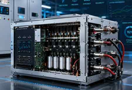
Modern defense operations depend on fast, reliable access to data in environments where standard storage devices are unlikely to perform consistently. Systems used in aircraft, naval vessels, armored vehicles and portable field equipment must withstand shock, vibration, extreme temperatures and constant movement.

To meet these demands, rugged military SSD manufacturers build storage solutions designed for durability, security and reliable performance. Their work goes beyond producing hardware, with extensive testing and engineering to meet strict defense standards. As military systems process more data, rugged solid-state storage has become a vital part of communication, surveillance and other mission-critical operations.

Selecting Silicon-Proven Memory IP for Advanced Semiconductor Design

Selecting Silicon-Proven Memory IP for Advanced Semiconductor Design

The semiconductor industry faces mounting pressure to deliver higher performance while controlling development costs. Process node transitions promise measurable improvements but require significant capital investment and extended qualification cycles. Executives responsible for acquiring memory intellectual property increasingly examine whether architectural refinement can deliver measurable gains without forcing immediate migration to smaller geometries. Memory subsystems influence performance, power consumption and silicon footprint across the entire chip. A poorly optimized memory block can limit system throughput, increase thermal load or complicate layout integration across complex system-on-chip designs.

Selecting Rugged Military SSD Drives for Defense Programs

Selecting Rugged Military SSD Drives for Defense Programs

Procurement mistakes in rugged military SSD drives rarely show up as a single failed part on a bench. They surface in qualification retests and program delays after storage has already been assigned to an avionics bay or mission computer. The device may be small; the penalty is not. For defense and aerospace executives, buying rugged storage is less a comparison of capacity and price than a judgment about the engineering control and configuration evidence needed behind a component expected to preserve data through vibration, heat exposure, cold starts and security-sensitive handling.

Reshaping Advanced Manufacturing with Semiconductor Test and Robotic Solutions

Reshaping Advanced Manufacturing with Semiconductor Test and Robotic Solutions

The semiconductor industry is at a point where precision, speed and adaptability are what make companies competitive. Manufacturers can not just rely on how much they can produce to stay relevant. They need automation, advanced testing environments and robots that can work together to handle very small and complex things. As chips get smaller and more powerful, even small mistakes during manufacturing can make them not work well, use much energy or not last long. So semiconductor test and robotic solutions are now a part of advanced electronics manufacturing.

Architecting the Future: Strategic Impact of AI-Driven Chip Design Automation

Architecting the Future: Strategic Impact of AI-Driven Chip Design Automation

The semiconductor industry stands at a transformative inflection point where complexity, performance demands, and cost pressures converge. Traditional chip design methodologies struggle to keep pace with the rapid evolution of applications such as artificial intelligence, edge computing, 5G/6G, automotive systems, and advanced computing. AI-driven chip design automation, where ML, generative models, and advanced optimization engines augment every stage of the design lifecycle, has emerged as a strategic game changer.

Rethinking Chip Design through AI-Driven Automation

Rethinking Chip Design through AI-Driven Automation

The semiconductor industry has reached a point where incremental gains in silicon no longer define competitive advantage; engineering velocity does. Chip development remains constrained by fragmented workflows, long verification cycles and manual iteration across specification, RTL and validation layers. These delays are not rooted in technical impossibility but in the inefficiencies of how work is coordinated.

Enhancing Chip Design Efficiency with High-Performance Memory IP Solutions

Enhancing Chip Design Efficiency with High-Performance Memory IP Solutions

Silicon-proven memory IP solutions are becoming essential strategic assets for semiconductor innovators, enabling accelerated time-to-market, optimized performance, and reduced design risk in advanced systems-on-chip and SoC architectures. As semiconductor complexity continues to escalate, the design and integration of memory subsystems remain among the most critical challenges in chip development. Memory interfaces, controllers, caches, PHYs (physical interfaces), and embedded SRAM or flash blocks contribute significantly to performance, power, and area metrics.