
Thank you for Subscribing to Semiconductor Review Weekly Brief
× 
Semi Conductor Review Weekly Brief
Be first to read the latest tech news, Industry Leader's Insights, and CIO interviews of medium and large enterprises exclusively from Semi Conductor Review
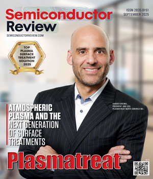
Plasmatreat has been recognized by Semiconductor Review Magazine as “Top Plasma Surface Treatment Solution 2025” based on our proprietary methodology, reflecting its position in the industry. This profile has been developed by the Semiconductor Review research and editorial team based on insights from an interview with Hardev Grewal, President and CEO.



Plasmatreat
Atmospheric Plasma and the Next Generation of Surface Treatments

 Hardev Grewal, President and CEO
The semiconductor industry relies on vacuum chambers for plasma surface treatment because the method is proven, effective, and well established. However, the model comes at a cost: high capital investment, complex infrastructure, limited throughput, and minimal flexibility for inline production. As devices shrink and become more sensitive, these trade-offs intensify.
Technical inertia is not the only barrier. Many engineers believe plasma can only exist in a vacuum, while atmospheric pressure plasma (APP) use damages delicate surfaces or produces harmful byproducts such as ozone.
These perceptions have slowed the adoption of alternatives, even as the need for faster, cleaner, and safer processes grows urgent.
The future of surface treatment requires breaking these assumptions, and Plasmatreat is leading the shift with its atmospheric plasma solutions that operate in open air, eliminate costly vacuum infrastructure, and increase throughput. Its Openair-Plasma® technology provides manufacturers with inline processing capabilities ideally suited for highly sensitive electronic components, efficiently replacing vacuum chambers and wet chemical cleaning in chip packaging. Beyond its technical advantages, the technology also introduces an environmental benefit. By replacing chemicals and reducing energy demands, it makes production cleaner, safer, and more sustainable, setting a new benchmark for the industry.
“Our technology has a small carbon footprint, uses a zero-potential plasma jet, and produces no harmful byproducts such as ozone. From wafer-level treatments to AI-driven packaging, power modules, and final assemblies, we enable innovation across the entire electronics spectrum rather than a narrow niche,” says Hardev Grewal, president and CEO.
Plasma Power without the Vacuum Chamber
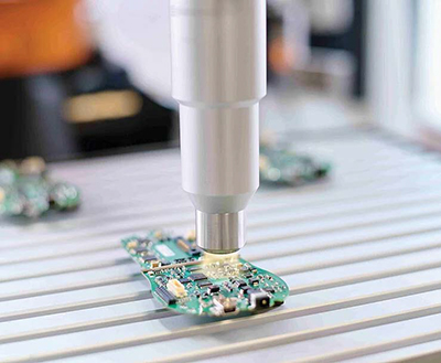
Plasmatreat’s Openair-Plasma® technology delivers surface treatment solutions that meet the rigorous requirements of modern manufacturing. Operating at atmospheric pressure, the system prepares surfaces for bonding, coating, and printing by generating plasma through the ionization of clean, compressed air using electrical discharge. The plasma jet system consists of a generator and an Industry 4.0-ready control unit, enabling precise adjustment of process parameters. Power and flow rate are continuously monitored to ensure consistency. Plasma is generated upstream of the jet nozzle, activating air that removes organic micro-contaminants and functionalizes surfaces. Unlike vacuum plasma methods, Openair-Plasma® enables area-selective treatment, allowing manufacturers to activate only the required zones while reducing chemical use, energy consumption, and cycle time. These capabilities are increasingly vital in semiconductor packaging.
-
These advantages have contributed to the widespread adoption of our plasma-based processes in thermal compression bonding, underfill, and oxide reduction applications. The equipment offers a significant cost advantage, with atmospheric plasma systems requiring only a fraction of the capital investment compared to traditional vacuum plasma machines
The industry is shifting from traditional single-chip wire bonding toward hybrid bonding, wafer-level packaging, and panel-level packaging that integrate multiple chips on larger substrates. These processes are especially critical for high-density AI applications. To meet these needs, Plasmatreat has developed advanced plasma jets capable of treating full wafer surfaces up to 300 mm and beyond, compared to earlier jets that treated only 4 to 10 mm widths. This scalability enables efficient, uniform pretreatment for wafer-level and panel-level packaging, supporting next-generation semiconductor manufacturing.
The Oxide Eraser for Clean, Bondable Surfaces
Uniform surface activation is only part of the equation. For reliable bonds, manufacturers must also address oxide layers that compromise adhesion. Traditional solutions such as formic acid treatments remove these layers but create significant drawbacks, including chemical waste, unstable surfaces, and the need for immediate downstream processing. Plasmatreat’s REDOX®-Tool offers a breakthrough alternative. Using inline plasma technology, it removes oxide layers while simultaneously activating surfaces for stronger bonds without harsh chemicals. The REDOX®-Tool leverages Openair-Plasma® technology in a controlled tunnel system with nitrogen and hydrogen to achieve flux-free bonding and selective oxide reduction without damaging the underlying metal.
Chemical approaches often leave unstable copper oxide surfaces prone to rapid reoxidation, but Plasmatreat’s method transforms the surface into a stable form that remains protected and eliminates the need for immediate downstream processing. The process is divided into three zones: pre-heating, plasma reduction, and cooling to ensure precise, reliable results for copper, nickel, and other metal oxides. This innovation directly addresses the challenges of advanced packaging, including miniaturization, reduced bump pitch, and flux residue, while lowering power consumption in demanding applications such as AI devices and co-packaged optics. By delivering a stable, clean surface through an environmentally friendly inline process, the REDOX®-Tool sets a new standard for quality, efficiency, and sustainability in semiconductor and IGBT manufacturing.
When Water Meets Plasma
Minimizing Environmental Footprint While Lowering Costs
Plasmatreat has advanced its technology beyond standard cleaning to include environmentally friendly metal oxide reduction. Its latest breakthrough is HydroPlasma®, a process that combines the effects of Openair-Plasma® with the chemical reactivity of water molecules to deliver a new way of cleaning surfaces. HydroPlasma® works by introducing water into the plasma process, where it is ionized to create highly reactive water molecules. These molecules act like soap, breaking down stubborn contaminants without harsh chemicals. The plasma-activated water stream is applied through a specially designed nozzle, effectively removing both organic residues such as oils and greases and inorganic contaminants such as salts. These are transformed into soluble or gaseous components, leaving surfaces thoroughly clean. This makes the technology especially promising for semiconductor packaging and other industrial applications. With no chemical waste and broad industrial potential, HydroPlasma® represents the next step forward in surface treatment technology.
 Tailored Nanocoatings with Precision Performance
Extending its advances in plasma technology, Plasmatreat has pushed the boundaries of surface engineering within the semiconductor industry, where nanocoatings play a critical role in chip production. The company has pioneered a breakthrough technology that enables nanocoatings to be applied under atmospheric conditions. Traditional methods rely on vacuum chambers, but this innovation applies precursor fluids within Plasmatreat’s atmospheric plasma jets to perform chemical vapor deposition directly in open air. By adjusting the precursor fluid, the coatings can be tailored to exhibit desired properties such as hydrophobicity, hydrophilicity, isolation, moisture barriers, corrosion resistance, or enhanced adhesion.
One of the most impactful applications of this capability is the selective application of dielectric barrier coatings to electronic devices. This approach delivers superior anti-corrosion protection for batteries, flexible electronics, and other sensitive components. While printed circuit boards have traditionally relied on broad conformal coatings for protection, Plasmatreat’s method combines the precision of area-specific chemical vapor deposition with the efficiency of atmospheric plasma. The result is targeted nanocoating for compact, complex devices, supporting the next generation of technologies such as augmented reality and virtual reality systems.
Our technology has a small carbon footprint, uses a zero-potential plasma jet, and produces no harmful byproducts such as ozone. From wafer-level treatments to AI-driven packaging, power modules, and final assemblies, we enable innovation across the entire electronics spectrum rather than a narrow niche
Minimizing Environmental Footprint While Lowering Costs
The benefits of these technologies extend beyond performance by reshaping how manufacturers view environmental responsibility. Plasmatreat combines advanced surface treatment innovations with a focus on sustainability, enabling manufacturers to achieve high-precision cleaning without harmful chemicals. Through global application labs and three dedicated R&D centers, the company collaborates closely with customers to co-develop solutions. This partnership model has earned the trust of leading semiconductor manufacturers and IDMs, particularly as Plasmatreat has helped them transition away from environmentally harmful cleaning methods such as formic acid baths that have dominated chip packaging for decades. This shift reduces environmental impact while lowering factory footprint, operating costs, abatement expenses, and waste management. At the same time, it delivers a more reliable and precise cleaning process that is proving to be a game changer in semiconductor production.
“These advantages have contributed to the widespread adoption of our plasma-based processes in thermal compression bonding, underfill, and oxide reduction applications. The equipment offers a significant cost advantage, with atmospheric plasma systems requiring only a fraction of the capital investment compared to traditional vacuum plasma machines,” says Grewal.
Global Expansion through Strategic Partnerships
For over 30 years, Plasmatreat has advanced atmospheric plasma solutions across industries including electronics, automotive, aerospace, life sciences, medical devices, transportation, and satellites. Headquartered in Germany, the family-owned company has grown into a global organization, operating 25 subsidiaries in 18 countries with offices in key manufacturing hubs worldwide. Its innovation centers in regions such as Silicon Valley, Phoenix, Japan, Singapore, Taiwan, and China serve as collaborative spaces where teams work directly with customers to test, demonstrate, and refine plasma technologies.
As electronics production shifts from China to Vietnam and India, Plasmatreat continues to expand globally, ensuring proximity to customers and building trusted partnerships that range from startups to Fortune 500 manufacturers. This growth is driven by a focus on relationships and problem-solving. The company prioritizes long-term customer success over short-term gains and extends this philosophy to its employees and product development. To meet the growing demand for integrated solutions, Plasmatreat collaborates with OEM partners, combining plasma cleaning systems with chip bonding technology to deliver high-performance results. This collaborative approach ensures every project benefits from shared expertise and a commitment to excellence.
Looking ahead, the company is well positioned to expand into emerging electronics and semiconductor manufacturing hubs. By aligning its presence with the geographic growth of customers, the company ensures that its expertise, technologies, and partnerships continue to drive innovation in advanced packaging, wafer-level processing, and AI-enabled electronics.
This combination of global reach and technical breakthroughs in Plasmatreat’s ability to replace vacuum chambers and harsh chemicals from plasma processes positions the company as a catalyst for the industry’s future. Its atmospheric solutions combine speed, precision, and sustainability, qualities that are increasingly vital as devices grow smaller and more complex. By overturning long-held assumptions about plasma, Plasmatreat is not only meeting today’s challenges but also enabling cleaner, faster, and more flexible production that the industry’s future depends on.
| Share this Article:Tweet
|
Company
Plasmatreat
Management
Hardev Grewal, President and CEO
Description
Plasmatreat is a global leader in atmospheric plasma technology that operates in 25 subsidiaries globally with offices in major manufacturing hubs. With patented Openair-Plasma® and functional coatings processes, the company offers high-performance solutions for cleaning, activation, and nanocoating to reduce chemical use and energy consumption in various industries.
This content is copyright protected
However, if you would like to share the information in this article, you may use the link below: