
Thank you for Subscribing to Semiconductor Review Weekly Brief
× 
Semi Conductor Review Weekly Brief
Be first to read the latest tech news, Industry Leader's Insights, and CIO interviews of medium and large enterprises exclusively from Semi Conductor Review
TECHNOORG LINDA has been recognized by Semiconductor Review Magazine as “Top 20 Semiconductor Tech Companies in Europe - 2023” based on our proprietary methodology, reflecting its position in the industry. This profile has been developed by the Semiconductor Review research and editorial team based on insights from an interview with András Szigethy, CEO.



TECHNOORG LINDA
Discover the Invisible

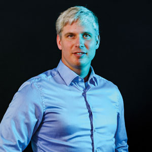 András Szigethy, CEO
Technoorg Linda, the Hungary-based scientific developer has long been pioneering in the field of ion milling and sample polishing for electron microscopy applications. They carved out a significant market both in SEM and TEM sample preparation and their technological maturity starts to show. With a bright future ahead of them, CEO András Szigethy speaks about new devices, applications and scientific territories yet uncharted by ion beam techniques.
A strangely inverse phenomenon can be observed for semiconductors: as products shrink, the market for them increases. With high demand for faster and smaller devices than ever before, the challenge has become observing the nano-sized building blocks.
Every atom needs to be accounted for. At this scale, we face a different challenge: are we looking at the true representation of our structures?


How can we be certain that sample preparation did not interfere with results, giving us a skewed concept of what lies within?
In a field where excellence prevails, there is no place for errors and uncertainty. "Finding answers to these questions and thus discovering the invisible is at the core of what Technoorg Linda does," elaborates András Szigethy, CEO of Technoorg Linda Co. Ltd.
Versatile Ion Beams
In the semiconductor field and at the forefront of material science, it has become paramount to remove the damage caused by mechanical or focused ion beam (FIB) sample preparations that precede imaging. An additional sample preparation step is required to remove the artifacts of grinding and polishing, as well as the artifacts of the high-energy bombardment of gallium ions during FIB lamellae preparation. The technology with the widest range of applications in this regard is broad ion beam (BIB) milling with argon ions. As proof of versatility, BIB is used in both scanning and transmission electron microscopy imaging (SEM and TEM, respectively).
“Keeping up with the latest trends in microscopy is key to our success. By focusing on both SEM and TEM, we can stay ahead of the application needs of our customers. For example, when talking about the semiconductor business, we have complete workflows dedicated to preparing samples of all sizes. This can range from revealing the atomic structures of groundbreaking new materials, to complex macroscopic structures like failure detection during system-on-chip manufacturing. With such a range of applications, we provide solutions for both academia and industry,” says Mr. Szigethy. 
"In addition to satisfying the needs of our result-focused users, we also have to aim at creating ready-to-go workflows and 'single-button' sample preparation solutions. In the busy semiconductor industry, personnel need to be able to learn to operate our devices quickly with results that meet expectations. Our mission has been to ensure that any technician can use our devices, and our control software's design reflects this belief. You set the sample milling parameters and press start."
A small dislocation loop is observed in GaN. Such dislocation loops are formed due to radiation damage; however, they are very small (< 5 nm) and can only be imaged if the sample thickness is comparable to their size. This section is less than 10 nm thick; in addition, it is very clean and free from damaged layers, making the imaging of such details possible. It was finished with Technoorg Linda’s low-energy argon ion source at 300 eV.
• Preparared with: Thermo Scientific Scios 2 Dual-Beam FIB SEM
• Imaged on: Thermo Scientific Titan Themis 200 Image Cs Corrected Transmission Electron Microscope
This philosophy holds true for Technoorg Linda's newest product, the SEM-mounted low-energy ion source known as LEGtoSEM.
Simply put, LEGtoSEM removes the artifacts of FIB lamella creation, including gallium implantation. By integrating the low-energy ion beam's gentle cleaning effect inside the dual-beam SEM, the need for a separate desktop device has also been eliminated. Now you can observe the cleaning's effect without the risky transportation of your fragile FIB lamella.
Trailblazers of Imaging
"In our more than three-decade-long history, our clear goal has been to perfect sample cleaning beyond the limits of possibility. Our main focus has been on developing tomorrow's solutions and achieving breakthroughs that could provide new possibilities and dimensions for our partners.
This idea has guided us over these years and defines the character of Technoorg Linda Co. Ltd.," adds the CEO.
The company has a lot of experience with preparing difficult samples as well. “We pushed what is possible with the technology by focusing on historically challenging samples: heat sensitive samples, multicomponent materials, cross-sections of thin films and coatings. Therefore, our products are present in the fields of metallurgy, geology, battery manufacturing, failure analysis, etc. The triumph of our precision was when we managed to cut through a Li battery separator foil with single-micron precision and without causing any heat damage (shown on the first page of the article). A lot of our recent technological advancements culminated in that single cross-section,” says Mr. Szigethy.
Technoorg Linda contributed to history by achieving scientific breakthroughs in the field of EM imaging. An early example is from the 90’s when their low-energy ion source was used to first image damage-free atomic lattices. More recent success is seen in Figure 2, showing a dislocation loop in an irradiated GaN sample.
-
In our more than three-decade-long history, our clear goal has been to perfect sample cleaning beyond the limits of possibility
The company has a lot of experience with preparing difficult samples as well. “We pushed what is possible with the technology by focusing on historically challenging samples: heat sensitive samples, multicomponent materials, cross-sections of thin films and coatings. Therefore, our products are present in the fields of metallurgy, geology, battery manufacturing, failure analysis, etc. The triumph of our precision was when we managed to cut through a Li battery separator foil with single-micron precision and without causing any heat damage (shown on the first page of the article). A lot of our recent technological advancements culminated in that single cross-section,” says Mr. Szigethy.
Looking for the Challenge
"We are in a great position. The new generation of our team has inherited a valuable tradition of focusing on real problems and attempting to solve the unsolvable. Every day, we dedicate ourselves to maintaining the flexibility and knowledge-based instrument development as the true path toward meeting users' expectations and real needs. Just as our team pioneered the development of dedicated tools for the low-energy range and made the observation of amorphous-free and artifact-free atomic structures possible, we are hard at work on achieving similarly significant milestones. Our new in-situ cleaning solution, LEGtoSEM, appears to be the next such milestone that the semiconductor industry has been waiting for," adds Mr. Szigethy.
"The rapid growth of the company demonstrates that focusing on innovation, maintaining flexibility, and building and nurturing a dedicated team will always pay off. In conclusion, a combination of these factors propels us forward to dream bigger, work more passionately, and provide the world with something that makes a real difference."
| Share this Article:Tweet
|

Company
TECHNOORG LINDA
Management
András Szigethy, CEO
Description
TECHNOORG LINDA operates in nanotechnology fields with a focus on developing and manufacturing ion technology-based instruments for extended use in specimen preparation and depth profiling connected to transmission and scanning electron microscopy.
This content is copyright protected
However, if you would like to share the information in this article, you may use the link below: