
Thank you for Subscribing to Semiconductor Review Weekly Brief
× 
Semi Conductor Review Weekly Brief
Be first to read the latest tech news, Industry Leader's Insights, and CIO interviews of medium and large enterprises exclusively from Semi Conductor Review
SCREEN has been recognized by Semiconductor Review Magazine as “Top 10 Semiconductor Manufacturing Solutions Companies in Europe - 2022” based on our proprietary methodology, reflecting its position in the industry. This profile has been developed by the Semiconductor Review research and editorial team based on insights from an interview with Yoshihide Higaki, Senior Marketing Executive & Dr. Martin Hollfelder Senior Director Technology & Service.



SCREEN
Semiconductor Innovation Inspired by Environmental Sustainability

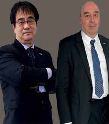 Yoshihide Higaki, Senior Marketing Executive & Dr. Martin Hollfelder Senior Director Technology & Service
Consider the following hurdle faced by manufacturers within the semiconductor industry as the horizontal scaling of semiconductor devices slows down, device structures become more three-dimensional than ever. The proposition supplements the fact that the diversification of semiconductor devices and electronics requires unique solutions for the production of each device, characterized by configuration, area, application, energy utilization, and various other use-case-specific parameters. As a collective outcome, the need for heterogeneous integration of technologies in high-performance packages, starting with those for deep learning and other machine learning systems, is at an all-time high within the semiconductor space. Likewise, creating links between chips necessitate sophisticated position measurement of all chips and flexible rectification. In this regard, SCREEN manufactures a wide range of wet clean/etch equipment to facilitate cutting-edge node manufacturing functions for logic and memory, trailing node manufacturing for analog, power, and CMOS sensors, and other electronic devices such as MEMS, SAW filters, and LEDs.
 “We continue to hold the largest market share in the wet clean/etch equipment, having been ranked #7 in the world for our semiconductor equipment from a revenue perspective and is recognized for its high quality,” explains Yoshihide Higaki, Senior Marketing Executive, SCREEN Semiconductor Solutions.
In addition to developing wet clean/etch equipment, the firm houses unique technologies and equipment for photoresist processing, wafer annealing, wafer inspection, and film thickness measurement. The equipment developed by SCREEN aids in the high-precision cleaning and processing of minute patterns in confined/limited spaces, thereby reducing the horizontal scaling of semiconductor devices. Clients can employ the firm’s cleaning technology developed to achieve larger production yields and high productivity. As device structures have begun adopting three-dimensional models, the firm focuses on developing new solutions that could assist its clients in cleaning and drying fragile semiconductors. It also sets the necessary groundwork for clients to develop advanced architectures through innovative wet etch technology.
Commandeered by SCREEN is also the Frontier Project, which develops and provides solutions for thin Si wafers and other materials such as sapphire, GaN, SiC, LiTa, LiNb, and AlTiC. In addition to its flagship 300 mm equipment, the company has birthed an extensive lineup of equipment through this initiative. The 300 mm systems are designed to deliver superior functionality and productivity, as necessitated by the advanced semiconductor marketplace; on the other hand, the Frontier series ensures the efficient handling of various substrate sizes and materials of 200 mm or smaller, crafted for the IoT space.
In the same light, SCREEN equips clients with unique anneal technology using xenon lamps, thereby drastically improving transistor performance.
 For extreme ultraviolet (EUV) lithography, the company is also working with consortiums and material manufacturers to develop processes that contribute to improved process stability, and to improve productivity using the world’s first “dual-track coating/developing system.” EUV lithography is an indispensable technology for the miniaturization of semiconductor devices. “For next-generation EUV lithography, we have partnered with a well-known Japanese paper company to develop a new photoresist chemical using hemicellulose. Hemicellulose is a plant-derived material, and through this collaboration, we hope to meet industry requirements for process performance and environmental impact,” says Mr. Higaki.
We continue to hold the largest market share in the wet clean/etch equipment, having been ranked #7 in the world for its semiconductor equipment in terms of revenue generated
In the manufacture of equipment, innovative manufacturing practices housed within its S3-3 manufacturing plant, which has successfully helped SCREEN increase its production efficiency by 1.5. Operational since 2019, the manufacturing facility features automated overhead transportation and automated stockers, which were built in response to the semiconductor shortage witnessed in recent years. SCREEN aspires to erect yet another manufacturing plant (S3-4) with the same objective by January 2023.
While these distinct manufacturing advantages speak volumes of the company’s technological competence, SCREEN’s prowess in catering to clients’ needs was demonstrated when the firm delivered a wide range of cleaning systems essential to semiconductor device manufacturing for TSMC.
With plans for a major production capacity expansion, TSMC required a reliable semiconductor solutions provider for varied applications. SCREEN’s effort enabled TSMC to stay on target by providing the necessary equipment with a minimal lead time. Furthermore, despite the ongoing COVID-19 pandemic, SCREEN enabled the localization of resources required for system installation and modification while allowing TSMC to scale up its advanced device manufacturing lines as per schedule. The successful partnership was a testament to the firm’s passion for walking the extra mile for client satisfaction.
The company can support remotely customers with augmented reality (AR). The project was developed in Europe with many customers operating in the semiconductor foundry business. With the support of advanced software and hardware (HMD, head-mounted device), AR-based remote support provides precise guidance in difficult tasks, such as during complex equipment installation and maintenance. The enablement of AR-based remote support has been demonstrated to be dramatically important and effective during the recent pandemic.
 As a signatory to the United Nations Global Compact, the firm is fully committed to meeting and exceeding the Sustainable Development Goals (SDGs). With these collaborations, SCREEN has set its sights on reducing the use of water, chemicals, and power, developing environmentally friendly solutions for its clients. The firm aspires to gradually contribute to the growth of the broader industry as a leading manufacturer of semiconductor cleaning equipment while trying to address the unique demands of each client. Engaging with businesses in the IoT, artificial intelligence, robotics, and 5G technologies, SCREEN’s push toward the highest sustainability standards is backed by the humble goal of serving humanity at large.
With businesses demanding advanced semiconductor manufacturing and eco-friendly solutions, SCREEN collaborates with leading semiconductor technology development centres such as imec, LETI, and AMAT META to provide sustainable, innovative solutions in the areas of wet clean/etch, photoresist processing, and annealing for advanced semiconductor manufacturing.
-
For next-generation EUV lithography, we have partnered with a well-known Japanese paper company to develop a new photoresist chemical using hemicellulose. Through this collaboration we hope to meet industry requirements for process performance and environmental impact
As a signatory to the United Nations Global Compact, the firm is fully committed to meeting and exceeding the Sustainable Development Goals (SDGs). With these collaborations, SCREEN has set its sights on reducing the use of water, chemicals, and power, developing environmentally friendly solutions for its clients. The firm aspires to gradually contribute to the growth of the broader industry as a leading manufacturer of semiconductor cleaning equipment while trying to address the unique demands of each client. Engaging with businesses in the IoT, artificial intelligence, robotics, and 5G technologies, SCREEN’s push toward the highest sustainability standards is backed by the humble goal of serving humanity at large.
As a company that firmly adheres to the Kyoto Protocol, which aims to cut down harmful emissions of gasses that fuel global warming, SCREEN lives and breathes sustainability. SCREEN’s 79 years of headquartering in Kyoto is indicative of several such environment-friendly initiatives overseen by the company. Observing the road taken thus far, alongside its developmental plans for the near future, SCREEN prepares for an eventful future with purpose-driven semiconductor solutions backed by an innovative spirit and the overarching goal of environmental sustainability.
| Share this Article:Tweet
|
Company
SCREEN
Management
Yoshihide Higaki, Senior Marketing Executive & Dr. Martin Hollfelder Senior Director Technology & Service
Description Read the success story from SCREEN Semiconductor Solutions Co., Ltd. Shifting To E-Mobility For A “Climate-Neutral Continent”: Sic-Based Power Electronics
SCREEN Semiconductor Solutions Co., Ltd manufactures a wide range of wet clean/etch equipment for cutting-edge node manufacturing such as logic and memory, trailing node manufacturing such as analog, power, CMOS sensor, and other electronic devices such as MEMS, SAW filters, and LEDs
This content is copyright protected
However, if you would like to share the information in this article, you may use the link below: