
Thank you for Subscribing to Semiconductor Review Weekly Brief
× 
Semi Conductor Review Weekly Brief
Be first to read the latest tech news, Industry Leader's Insights, and CIO interviews of medium and large enterprises exclusively from Semi Conductor Review
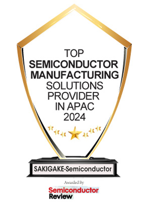
SAKIGAKE-Semiconductor has been recognized by Semiconductor Review Magazine as “Top 10 Semiconductor Manufacturing Solutions Provider In Apac - 2024” based on our proprietary methodology, reflecting its position in the industry. This profile has been developed by the Semiconductor Review research and editorial team based on insights from an interview with Mahiro Fukumori, Leader of the General Affairs Department.



SAKIGAKE-Semiconductor
The Leader in Plasma Technology Innovation

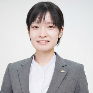 Mahiro Fukumori, Leader of the General Affairs Department
It offers a wide array of equipment tailored for research and development purposes as well as large-scale production, catering to various stages of technological advancement and production scale.
“Our extensive range, backed by numerous awards and a longstanding track record of customer satisfaction, guarantees support for every phase of operations,” says Kohshi Taguchi, CEO of SAKIGAKE-Semiconductor.
From semiconductor and electronic component to precision equipment and medical product manufacturers, everyone rely on SAKIGAKE-Semiconductor’s innovations for driving advancements and ensuring higher standards and better outcomes. For instance, its pretreatment equipment application for wire bonding improves surface cleanliness and adhesion, and mold material removal equipment facilitates rapid and accurate defect analysis.
In biotechnology, SAKIGAKE-Semiconductor’s cell culture pretreatment boosts efficiency and accuracy. For contact lens manufacturing, it ensures high product reliability through superior surface treatment. Additionally, the company’s technology advances various medical product manufacturing processes, improving efficiency and quality.
Pioneering Long-Term Surface Modification Solutions
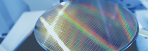 SAKIGAKE-Semiconductor ensures the longevity and effectiveness of surface modification properties. The development and invention of advanced technologies, such as forming self-assembled monolayers (SAM) using plasma-enhanced molecular bond formation (PE-MBF), are prime examples. This technology ensures the longevity of treatment effects, offering environmentally friendly and highly customizable solutions.
The innovative SAM using PE-MBF technology forms a high-density, stable monolayer on material surfaces, enabling long-term maintenance of modification properties.
This allows the self-assembly of high-density monolayers on material surfaces, providing precise control of surface chemistry and flexibility in adjusting surface hydrophilicity and water repellency.
Driving this customer-centric approach is a commitment to innovation. SAKIGAKE-Semiconductor integrates cutting-edge plasma technology into its equipment, achieving performance and efficiency that exceed industry standards. Continuous investment in research and development ensures state-of-the-art solutions that keep clients ahead of the competition.
PE-MBF employs plasma to enhance the strength of intermolecular bonds, leading to superior surface modifications. The method offers several advantages, including stronger bond formation, increased surface energy and environmental sustainability due to its dry process, which does not produce waste liquid.
SAKIGAKE-Semiconductor’s SAM formation technology guarantees the highest levels of plasma reproducibility and uniformity. All treatments, from plasma irradiation to reagent application, are conducted within the same vacuum chamber, ensuring consistent control and time reduction.
Tailored Solutions for Every Need
SAKIGAKE-Semiconductor recognizes the uniqueness of each project. Its team of experts closely works with clients to understand specific needs and deliver desired outcomes. The personalization optimizes the properties of treated surfaces for their intended applications, enhancing performance and extending longevity.
-
Our extensive range, backed by numerous awards and a longstanding track record of customer satisfaction, guarantees support for every phase of operations
Driving this customer-centric approach is a commitment to innovation. SAKIGAKE-Semiconductor integrates cutting-edge plasma technology into its equipment, achieving performance and efficiency that exceed industry standards. Continuous investment in research and development ensures state-of-the-art solutions that keep clients ahead of the competition.
One of its significant successes involved a semiconductor manufacturer striving to improve surface cleanliness and adhesion during the wire bonding pretreatment process. The implementation of the company’s advanced technology resulted in a dramatic increase in surface cleanliness. This improvement directly translated into stronger adhesion during the wire bonding process, ensuring a more reliable and durable bond.
Beyond adhesion strength, the streamlined treatment process developed by SAKIGAKE-Semiconductor increased production line throughput. By optimizing pretreatment steps, the manufacturer experienced enhanced overall manufacturing efficiency, reduced downtime and boosted productivity.
The advancement is a prime example of how SAKIGAKE-Semiconductor’s innovations yield real-world client benefits. One of SAKIGAKE-Semiconductor’s key advantages is its strategic location in Kyoto, a hub that draws top-tier talent. Additionally, the company features unique educational programs and career planning for employees, highlighting its commitment to valuing its people. Benefiting from its advantageous location and excellent workforce, it contributes to regional economic development and job creation.
SAKIGAKE-Semiconductor’s plasma technology differentiates itself as a sustainable initiative compared to traditional wet processes by simplifying processes and eliminating the need for waste liquid treatment. This commitment to sustainable technology and operations has earned SAKIGAKE-Semiconductor numerous awards for not only its new technologies but also its exemplary management practices.
The company’s innovations are transforming the semiconductor manufacturing industry. By enhancing adhesion strength, ensuring uniform droplet distribution and enabling rapid and precise defect analysis, it drives its clients’ success and growth to new heights. Its groundbreaking advancements are not just making a difference— they are setting a new standard of excellence in plasma equipment manufacturing. This is supported by the fact that the company has been featured hundreds of times in various media outlets since its inception.
| Share this Article:Tweet
|
Company
SAKIGAKE-Semiconductor
Management
Mahiro Fukumori, Leader of the General Affairs Department and Koshi Taguchi, CEO
Description
SAKIGAKE Semiconductor is a plasma equipment manufacturer in Kyoto, Japan, established in 2002 as a venture company from Kyoto Institute of Technology. The company develops, manufactures, and sells plasma equipment for surface treatment processing, primarily for the research and production departments of universities and major companies.
This content is copyright protected
However, if you would like to share the information in this article, you may use the link below: