


Thank you for Subscribing to Semiconductor Review Weekly Brief
× 
Semi Conductor Review Weekly Brief
Be first to read the latest tech news, Industry Leader's Insights, and CIO interviews of medium and large enterprises exclusively from Semi Conductor Review
Renesas Electronics Corporation has been recognized by Semiconductor Review Magazine as the exclusive recipient of “Top PCB Design Software 2026,” based on our proprietary methodology, reflecting its position in the industry, and is also named among “Top PCB Design Solutions,” reflecting its broader leadership. This profile has been developed by the Semiconductor Review research and editorial team based on insights from an interview with Leigh Gawne, VP, Head of R&D, Digital Industries.


The embedded engineering sector remains one of the last industries to adopt full digital modernization, with hardware, software, and system design still operating in siloed and fragmented domains. Renesas Electronics Corporation addresses that gap through Renesas 365, powered by Altium, bringing its Digitalization Vision into an intelligently integrated cloud-based environment that connects silicon to system.
Renesas 365 is a unified embedded system development platform that connects, rather than replaces, existing toolchains, integrating design intent, components, and workflows within a platform grounded in open-modeled components and contextual intelligence. Rather than forcing teams to reconcile separate environments late in development, it establishes digital continuity across domains from the outset.
Establishing a Unified Design State Across Domains
At the center of this shift is a shared and consistent design state. Concept definition, software development, and hardware design operate from a synchronized representation of the system, where intent carries across domains intelligently. Changes in one area are visible in others, allowing teams to identify design issues earlier, shift system integration left, and reduce rework.
 “We are reimagining the way embedded engineers go about designing software-defined products, bringing hardware, software, and system elements together across vendors to work as a unified ecosystem,” says Leigh Gawne, VP and Head of R&D, Digital Industries, at Renesas Electronics Corporation.
The need for that shift is rooted in day-to-day engineering reality. Embedded teams still spend significant time resolving version mismatches, locating the right documentation, and configuring tools and environments before their actual system design begins. Renesas 365 targets that non-value-added burden by shifting more of that heavy lifting into the platform through modeled components, contextual awareness, and scenario evaluation.
Designed as an open platform, its first implementation centers on the Renesas RA family of microcontrollers, with more than 550 MCU variants available within a model-based environment for system-aware exploration. Engineers begin by importing their existing projects or expressing design intent through freeform block diagrams in the Electronic System Designer, which the platform’s constraint modeling engine then interprets against modeled components to perform floor planning for on chip peripheral assignment and pin multiplexing, as well as additional capabilities such as power budgeting, memory consumption, and compute that will be available in the future.
That openness extends into lifecycle execution, an area Gawne describes as nascent for most embedded customers today. Drawing a parallel to how Product Lifecycle Management (PLM) and Mechanical Computer-Aided Design (MCAD) reshaped mechanical-centric product development in the 1980s and 90s, Renesas 365 introduces an embedded DevOps model in which design, deployment, and operation form a continuous loop.
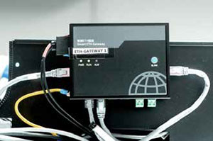 The platform also enables cross-probing between software and hardware domains, allowing a developer to navigate from a line of source code directly to a physical net or pin on the board. In the future, engineers can exercise what executives describe as the “power of what if,” evaluating configurations and exploring alternatives dynamically across power, memory, and performance constraints before committing to architectural decisions.
Extending into Open Ecosystems and Lifecycle Continuity
Altium’s platform is central to enabling this shift. Renesas contributes semiconductor and embedded expertise, while Altium brings mature, cloud-based collaboration and workflow infrastructure. Together, they form an engineering framework that connects design, collaboration, and lifecycle management in ways isolated tools simply cannot.
Renesas 365 is also positioned as an open participation model rather than a vendor-specific environment. Third-party components, solutions, tools, models, and contributors can operate within the same shared context, avoiding the fragmentation that typically arises across supply chains.
“Renesas 365 is built on open-platform concepts where every partner component and system solution is modeled for seamless integration, eliminating the burden of fragmented engineering research and unlocking a true ‘what if’ design paradigm that finally brings multiplicative innovation to the industry,” says Hooman Foroughi, VP and Head of Application and Software Engineering, Embedded Processing, at Renesas Electronics Corporation.
-
We are reimagining the way embedded engineers go about designing software-defined products, bringing hardware, software, and system elements together across vendors to work as a unified ecosystem.
That openness extends into lifecycle execution, an area Gawne describes as nascent for most embedded customers today. Drawing a parallel to how Product Lifecycle Management (PLM) and Mechanical Computer-Aided Design (MCAD) reshaped mechanical-centric product development in the 1980s and 90s, Renesas 365 introduces an embedded DevOps model in which design, deployment, and operation form a continuous loop.
With regulatory expectations such as the European Cyber Resilience Act shaping requirements for software-defined products in the field, version control, over-the-air updates, and lifecycle management keep systems aligned with their original design intent while adapting to new requirements.
“The true value of Renesas 365 is in freeing engineers from tedious and error-prone work — looking up data sheets, validating PCB routing, and translating requirements into algorithms and hardware. We let the platform handle much of that complexity, to free embedded architects and engineers to focus on their end application design value,” says Foroughi.
Renesas 365 shifts embedded engineering from disconnected workflows to a connected system where design intent, components, and lifecycle remain aligned, delivering earlier integration, reduced rework, and more predictable development.
Reframing PCB Design Software for System-Level Engineering
PCB design software has long been treated as a discrete step within a broader engineering workflow, focused on schematic capture, layout precision and manufacturability. That framing no longer holds under the weight of modern embedded systems, where software-defined functionality, connectivity requirements and component diversity introduce a level of interdependence that traditional tools were not built to manage. Engineering teams are no longer constrained by layout complexity alone; they are constrained by fragmentation across tools, domains and decision points that sit upstream and downstream of PCB design itself.
The most significant and ongoing problem is not necessarily the capability of the tools, but the lack of connectivity between the tools. Hardware designers, software engineers and system architects typically work in parallel domains that don't share a consistent model of design intention. Requirements are interpreted differently among domains, documentation is out of date and validation only occurs late, often during integration when corrections are costly.
This fragmentation is compounded by the diversity of applications in embedded systems. Each use case brings its own set of tools, workflows and dependencies, forcing teams to reconstruct their environment repeatedly. The result is a design process where value creation is delayed, iteration cycles are prolonged and decision-making is constrained by the effort required to evaluate alternatives. This prevents a "what if" exploration of possibilities and restricts system-level optimization opportunities.
A better model results when the PCB design is not treated as an independent task but rather as a step within the overall system model. In this model, design intent is captured early and expressed in a way that can be interpreted across domains. Component choices, system performance and requirements are explicitly described as data structure inputs to the subsequent design steps automatically. Instead of manually reconciling datasheets, tool outputs and design assumptions, engineers operate within an environment where context is shared and continuously updated.
This shift changes how teams assess PCB design software. The question is no longer whether a tool can perform layout tasks efficiently, but whether it can support a connected design process that spans concept development, component selection and system validation. The ability to take high-level design objectives and turn them into practical design configurations is becoming increasingly important. Just as important is maintaining alignment between hardware and software, ensuring that configuration states, dependencies and constraints remain consistent throughout the development process.
Time-to-market improvements come from this continuity rather than isolated efficiency gains. When design decisions are evaluated earlier and updated dynamically, the need for late-stage corrections is reduced. Iteration times shorten and become more reliable, allowing the team to progress confidently from idea to deliverable.
Renesas Electronics Corporation positions its Renesas 365 platform within this emerging model. It goes beyond traditional PCB design by bringing requirements, component data and design workflows into a single environment. By evaluating design requirements alongside available components, the platform helps engineers identify viable options more quickly and reduces the manual effort involved in assessing feasibility. Its approach links hardware and software through shared models, keeping configurations aligned and allowing teams to quickly adapt as requirements evolve.
The result is a design experience where engineers spend less time assembling tools and more time refining system behavior. Through continuity and the built-in context of the Renesas 365 workflow, PCB design is aligned more closely with the system-level requirements imposed on current embedded systems, making it a strong choice for organizations aiming to move from fragmented processes to coordinated system-level engineering.
...Read more
PCB Design Software Info
Q1
What Should Engineering Teams Expect From Modern PCB Design Platforms?
Modern PCB Design Software should do more than let engineers draw schematics and route boards. It should close the gaps between component selection, board layout, firmware development, documentation and design review. When these steps are scattered across disconnected files and tools, teams end up spending more time reconciling versions than solving real engineering problems. Strong platforms provide a more continuous path from early concept to manufacturable product, especially when hardware and embedded software decisions are tightly linked.
Q2
How Does Renesas Electronics Corporation Connect PCB Design Software to Embedded Development?
Renesas Electronics Corporation connects PCB Design Software more directly with embedded development through its ecosystem that combines Renesas devices, Altium technology and Renesas 365. After acquiring Altium, the company moved toward a more unified design environment that links silicon selection, hardware design and embedded software development. Renesas 365, powered by Altium, helps engineers move from device discovery and system aware MCU selection into schematic design and firmware work while keeping design context consistent across tools.
Q3
Why Does Cloud Collaboration Matter in Board Design?
PCB design is rarely a single engineer working in isolation anymore. Cloud enabled PCB Design Software makes it easier to manage design reviews, track changes, verify components and coordinate handoffs between hardware, firmware and product teams. This is especially important when multiple stakeholders need to work from the same up to date design source. Instead of exchanging files through email or local storage, teams can maintain a shared and traceable design record that reduces confusion when requirements evolve.
Q4
Which Evaluation Factors Matter in PCB Design Software?
A meaningful evaluation of PCB Design Software should focus on how it performs under real engineering conditions rather than only feature lists or demonstrations. Teams should assess schematic capture, layout capabilities, library management, version control, collaboration features, component data integration and manufacturing outputs. The best test is to run an actual board project through the workflow to see how the platform handles design iterations, review feedback and hardware software dependencies without introducing extra manual coordination overhead.
Q5
How Can Design Software Shorten the Path From Concept to Product?
PCB Design Software can accelerate development when it keeps early engineering decisions connected throughout the entire design process. Choices around components, power requirements, pin assignments and firmware assumptions often shape the final product long before layout is complete. A connected workflow helps identify mismatches earlier and reduces late stage redesign. It also allows teams to reuse validated design knowledge instead of rebuilding from scattered spreadsheets, outdated project folders or informal documentation.
Q6
What Makes Renesas Electronics Corporation Relevant to Electronics Design Teams?
Renesas Electronics Corporation is relevant to design teams because its PCB Design Software strategy is closely aligned with its broader semiconductor portfolio, which includes embedded processing, analog and connectivity, and power solutions. Its move toward standardized PCB development using Altium 365 reflects internal adoption rather than just external positioning. This connection between device selection, board design, embedded software and lifecycle data helps engineering teams maintain continuity from concept through production in a more structured and traceable way.
| Share this Article:Tweet
|
Company
Renesas Electronics Corporation
Management
Leigh Gawne, VP, Head of R&D, Digital Industries and Hooman Foroughi, VP, Head of Application and Software Engineering, Embedded Processing
Description
Renesas Electronics Corporation, a leading provider of advanced semiconductor solutions, acquired Altium, a global leader in electronic design systems, in August 2024. In March 2026, the two companies launched Renesas 365, an open platform that connects hardware, software, and system design through a unified silicon-to-system engineering model.
This content is copyright protected
However, if you would like to share the information in this article, you may use the link below:
https://www.semiconductorreview.com/renesas-electronics-corporation-2026