


Thank you for Subscribing to Semiconductor Review Weekly Brief
× 
Semi Conductor Review Weekly Brief
Be first to read the latest tech news, Industry Leader's Insights, and CIO interviews of medium and large enterprises exclusively from Semi Conductor Review
PseudolithIC has been recognized by Semiconductor Review Magazine as “Heterogeneous Integration Technology of the Year 2025” based on our proprietary methodology, reflecting its position in the industry. This profile has been developed by the Semiconductor Review research and editorial team based on insights from an interview with Florian Herrault, CEO and Co-founder.


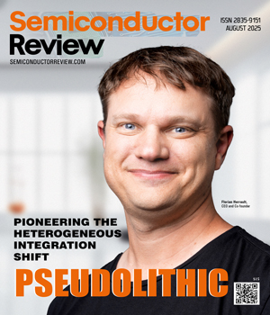
 Florian Herrault, CEO and Co-founder
PseudolithIC, a pioneer in heterogeneous integration, addresses this challenge with true chiplet-level integration on a common silicon CMOS wafer. By uniting diverse semiconductor materials and functionalities into a single platform, the company enables seamless and scalable transitions from monolithic architectures to modular, high-performance RF systems on a chip (RF SoC).
PseudolithIC is on a mission to commercialize cutting-edge compound semiconductor technologies, serving a wide range of markets—from wireless infrastructure and SATCOM to quantum computing and defense applications.
“Specializing in heterogeneous technology, we go beyond just combining different materials,” says Florian Herrault, CEO and co-founder. “Our IP revolves around both design and fabrication, leveraging the highest-performance transistors from leading-edge compound semiconductor foundries while developing intelligent circuits on a cost-effective silicon CMOS platform that can scale efficiently.”
The Perfect Blend of GaN and Silicon
Since cost is a major concern for businesses adopting heterogeneous integration, PseudolithIC offers a ready-made solution that doesn’t compromise on performance. The company has developed a digital and physical library of standardized chiplets made from compound semiconductor materials, significantly reducing prototyping expenses. Using these chiplets, it can design and test RF circuits in silicon in as little as three months—enabling faster iteration than traditional monolithic circuit technologies.
Building on this foundation, PseudolithIC’s next-generation RF and millimeter-wave chipsets incorporate silicon to further improve cost-efficiency. The precision of silicon transistor and passive element modeling ensures higher first-pass success rates in prototyping, enhancing overall productivity.
Through its 200-mm-diameter silicon platform, the company also addresses the high cost of GaN chips by integrating microscopic GaN transistor chiplets with CMOS technologies. At the same time, it maximizes yield by producing as many chiplets as possible from small-diameter compound semiconductor wafers. For instance, a four-inch GaN wafer can yield around 100,000 chiplets. While the number of chiplets per wafer increases, PseudolithIC designs final silicon solutions with as few chiplets as possible. This reduces overall product costs by using only small amounts of GaN (or InP or GaAs), with the majority of the circuit built from silicon.
-
Our IP revolves around both design and fabrication, leveraging the highest-performance transistors from leading-edge compound semiconductor foundries while developing intelligent circuits on a cost-effective silicon CMOS platform that can scale efficiently
Through its 200-mm-diameter silicon platform, the company also addresses the high cost of GaN chips by integrating microscopic GaN transistor chiplets with CMOS technologies. At the same time, it maximizes yield by producing as many chiplets as possible from small-diameter compound semiconductor wafers. For instance, a four-inch GaN wafer can yield around 100,000 chiplets. While the number of chiplets per wafer increases, PseudolithIC designs final silicon solutions with as few chiplets as possible. This reduces overall product costs by using only small amounts of GaN (or InP or GaAs), with the majority of the circuit built from silicon.
The silicon platform is also compatible with traditional packaging techniques such as copper bumping and 3D stacking, eliminating the need for costly new infrastructure—a key advantage of working with silicon.
Delivering More with Co-Integrated Chipsets
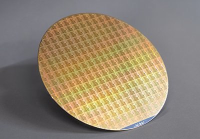 To further optimize cost and performance, PseudolithIC provides flexibility in mixing and matching different materials to optimize circuit designs. For instance, the company uses GaN in applications requiring high power and efficiency in the amplifier section. When low noise is essential in the receiver section, it employs indium phosphide for the low-noise amplifier (LNA), selecting the best material for each function within the circuit.
By integrating CMOS transistors alongside GaN, PseudolithIC delivers a balanced, high-performance solution. While GaN and silicon are widely used individually, they don’t offer the same level of integration or functionality as PseudolithIC’s heterogeneous technology. The company designs analog components in silicon, enabling capabilities not possible with silicon-only or GaN-only systems. This unique integration of CMOS with high-performance semiconductor materials on a single chip sets PseudolithIC apart.
A recent project illustrates this value: a phased array client turned to the company to reduce component costs and resolve design delays caused by the complexity of GaN integration. By co-integrating essential power management circuitry in silicon CMOS with GaN transistor chiplets on a single chip, PseudolithIC maintained the high-performance amplifier while streamlining system integration and operation—enabling smaller, cheaper, and more efficient phased arrays.
“Our clients come to us for complete product solutions—not just technology platforms or design kits—which drives us to deliver results from concept to execution,” says Herrault.
A Dual Approach to Excellence
To bring its products to market, the company employs two primary approaches. First, it offers a catalog model featuring ready-to-deploy solutions. Second, it engages directly with clients to address specific needs, including technology qualification, reliability, packaging, and product release processes.
One standout example of this tailored approach is how PseudolithIC addresses one of the biggest challenges in heterogeneous integration: thermal management—particularly with GaN, which can generate significant heat. To solve this, the company provides direct physical access to the backside of transistor chiplets, allowing a heat spreader to be attached directly. This approach delivers exceptionally low thermal resistance compared to competing technologies.
Future Product Lines
Looking ahead, PseudolithIC plans to release product samples for millimeter-wave power amplifiers, low-noise amplifiers, and transmit/receive front ends.
For transmit and receive applications, it is developing a range of chipsets covering frequencies from C to W-band (approximately 6 GHz to 86 GHz), tailored to meet the specific needs of various markets. These chipsets will deliver output powers ranging from 1 to 10 watts, with high efficiency and very low noise figures between 1.5 and 2.5 dB. For SATCOM, cellular backhaul, and long-range radar, the company is also developing receiver and transmitter solutions operating at 71–76 GHz and 81–86 GHz to deliver enhanced performance.
As PseudolithIC continues to lead in heterogeneous integration, its innovations are redefining semiconductor technology and transforming industries—from telecommunications to quantum computing. By combining compound semiconductor chiplets with large-diameter, low-cost silicon wafers, PseudolithIC is setting a new standard for high performance, power efficiency, and scalable RFIC solutions.
| Share this Article:Tweet
|
Company
PseudolithIC
Management
Florian Herrault, CEO and Co-founder
Description
PseudolithIC is a leader in semiconductor heterogeneous integration, transforming wireless communications and merging diverse semiconductor materials into single chips. Its solution offer the performance of a MMIC in an RFIC ecosystem yielding faster, cheaper and better performance than is possible with a monolithic approach.
This content is copyright protected
However, if you would like to share the information in this article, you may use the link below: