


Thank you for Subscribing to Semiconductor Review Weekly Brief
× 
Semi Conductor Review Weekly Brief
Be first to read the latest tech news, Industry Leader's Insights, and CIO interviews of medium and large enterprises exclusively from Semi Conductor Review
Nova Ltd. has been recognized by Semiconductor Review Magazine as “Top 10 Semiconductor Solutions Providers - 2024” based on our proprietary methodology, reflecting its position in the industry. This profile has been developed by the Semiconductor Review research and editorial team based on insights from an interview with Zohar Gil, CMO.


 Zohar Gil, CMO
In an interview with Semiconductor Review, Zohar Gil, CMO, discusses how Nova Ltd.'s innovative metrology solutions, crafted with precision, are transforming semiconductor manufacturing.
Can you please provide a brief overview of Nova Ltd.?
Nova Ltd. is a global provider of dimensional, materials, and chemical metrology solutions for advanced process control in semiconductor manufacturing. We bring versatile expertise and solutions to a wide range of device segments, from leading-edge logic to advanced memory, advanced packaging, and specialty devices. The world’s largest chip manufacturers deploy our solutions to drive faster times to market and higher yields at the most complex and advanced production lines, enabling them to stay ahead in an industry defined by constant evolution and increasing complexity.
We have a broad sales and services presence worldwide and three R&D centers in Israel, Germany, and the US.
What challenges do clients face, and how are you positioned to solve them?
The semiconductor industry is racing to keep up with the demand for faster, more powerful, and energy-efficient chips needed for AI applications, which is the main driver of the industry today. These demands are driving increasingly complex designs, both in architecture and materials.
-
The world’s largest chip manufacturers deploy our solutions to drive faster times to market and higher yields at the most complex and advanced production lines, enabling them to stay ahead in an industry defined by constant evolution and increasing complexity
As designs become more complex, novel process control techniques and capabilities, like measuring in-die, high aspect ratios, and at the wafer edge, become essential for process development and high-volume manufacturing. Our product portfolio blends precise hardware and smart software to give clients the insights they need to create cutting-edge semiconductor devices. Taking a fresh, innovative approach, we provide solutions that open new information channels and challenge traditional industry norms, making advanced IC manufacturing more efficient and effective.
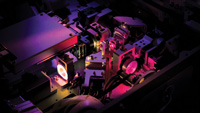 Nova Ltd. strategically categorizes its cutting-edge metrology solutions into three key offerings: dimensional, materials, and chemical metrology.
Boosting performance and power efficiency in IC devices starts with precise measurements—down to the nanometer and angstrom levels. That’s where our dimensional metrology solutions for process control come in. We offer two flexible configurations: Integrated and Standalone metrology.
Our compact Integrated metrology tools attach directly to manufacturing equipment, delivering near-100 percent sampling for tight process control, perfect for tasks like chemical-mechanical planarization. Meanwhile, our standalone systems work independently of specific tools, providing unmatched adaptability and precision for a variety of applications.
Our unique solution, the Nova Ltd. Prism platform, is an example of our dimensional metrology solutions. Customers are adopting backside power delivery designs in their logic chip manufacturing, utilizing advanced techniques like hybrid bonding, through-silicon via, and redistribution layers. The reason for using these complex processes is to achieve higher bandwidth, lower latency, and lower power to support the massive computational demands of AI model training and inferences. The Nova Ltd. Prism platform uses spectral interferometry technology with unique algorithms to deliver exceptional sensitivity and precision, extracting only the most relevant measurement parameters from extensive data.
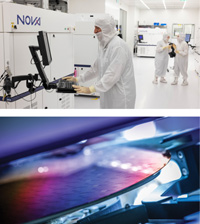 The architecture challenges I referenced earlier include an array of new materials, alloys, and compounds. To address these challenges, we offer materials metrology tools that measure key factors like thickness, composition, stress and strain. As advanced devices use more diverse materials, the need for precise measurement grows, driving our leadership and growth in this vital area.
Our materials metrology solutions are unique because these are lab-scale technologies that Nova Ltd. developed into fully automated, reliable solutions for high-volume semiconductor manufacturing. Our portfolio includes advanced technologies like X-ray, Raman spectroscopy, and Secondary Ion Mass Spectrometry (SIMS), all of which address the most acute challenges in materials measurements.
Nova Ltd.’s VeraFlex platform has become an industry standard for materials metrology. Using X-ray photoelectron spectroscopy (XPS) and X-ray fluorescence (XRF), these tools tackle challenges by precisely measuring complex material stacks. The platform is particularly effective at measuring the composition and thickness of intricate structures, offering more accuracy than traditional optical tools. For example, in advanced DRAM manufacturing, it provides precise measurements of dielectric capacitor layers, ensuring chip stability and performance in high-volume production, which in logic devices, VeraFlex analyzes complex high-K metal stacks, where precise material and dimensional measurements are critical.
Our chemical metrology solutions are just as impressive and play a crucial role in managing the chemical processes in semiconductor manufacturing across back-end wafer-level packaging, front-end dual-damascene process steps, and advanced substrate and PCB plating processes. Our advanced sensors and chemical metrology analysis techniques enable precise control over a wide range of chemical baths used for electrochemical deposition. The Baths’ chemical compositions and concentrations during production must be closely monitored to ensure high yields. This boosts performance and enhances cost-efficiency, especially with custom-formulated chemistries.
The patented Direct Metal Replenishment technology is one of Nova Ltd.’s innovations in chemical metrology. It offers economical replenishment of metals in a plating bath, significantly extending the bath chemicals’ lifetimes, improving plater utilization, and minimizing operational risks and costs.
How does Nova Ltd. drive efficiency and accuracy in semiconductor fabrication?
At Nova Ltd., innovation is at our core, fueled by strong investment in R&D to develop new technologies and improve existing products. Delivering unmatched precision and expertise, we’ve become a trusted partner for semiconductor manufacturers, providing them with advanced metrology solutions. Our talented team of experts drives our success and remains central to everything we do. We’re committed to supporting our employees, promoting diversity, prioritizing well-being and building a strong sense of community.
| Share this Article:Tweet
|

Company
Nova Ltd.
Management
Zohar Gil, CMO
Description
Nova delivers cutting-edge metrology solutions for semiconductor manufacturing, offering dimensional, materials and chemical metrology. Its high-precision tools drive operational efficiency and innovation, supporting advanced processes like 3D architectures, DRAM, and 3D NAND. With integrated and standalone configurations, Nova ensures precise measurements, enhancing performance, product yields, and reducing time-to-market.
This content is copyright protected
However, if you would like to share the information in this article, you may use the link below: