
Thank you for Subscribing to Semiconductor Review Weekly Brief
× 
Semi Conductor Review Weekly Brief
Be first to read the latest tech news, Industry Leader's Insights, and CIO interviews of medium and large enterprises exclusively from Semi Conductor Review
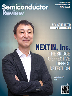
NEXTIN, Inc. has been recognized by Semiconductor Review Magazine as “Top 5 Semiconductor Companies in South Korea - 2022” based on our proprietary methodology, reflecting its position in the industry. This profile has been developed by the Semiconductor Review research and editorial team based on insights from an interview with Chris Park, CEO.



NEXTIN, Inc.
The Bridge to Effective Defect Detection

 Chris Park, CEO
Adding to the cost and performance factors, NEXTIN, Inc., an inspection solutions provider, brings in sensitivity measures to allow semiconductor manufacturers to automate the increased number of steps in modern optical inspection.
“We address the prevalent needs of our customers and deliver solutions critical for a wafer inspection system,” says Ram Segal, CTO at NextIn.

NextIn’s line of core inspection systems is in tune with the latest 2D and 3D printing operations of semiconductor production. This portfolio includes Aegis, a defect detection machine based on its innovative 2D imaging technology. Wafer manufacturers can identify and observe points on a chip susceptible to damage and find 1x-nm node semiconductor processing pattern defects. High sensitivity and throughput ensure Aegis finds issues like gaps in bridges, thinning, protrusion, footing in ion implantation, cleaning, and film scratches and particles at a very low false alarm and nuisance rate. Support for 200mm and 300mm size semiconductors guarantees Aegis is compatible across many manufacturing applications.
Further, NextIn’s unique patents allow for a combination of high defect capture rate and throughput, enabling clients to substantially lower production costs. An attractive solution for tracking challenges in most logic and memory devices, Aegis includes a list of patents related to system design, detection algorithms and AI for the automatic defect classification of wafer inspection.
Specializing in developing unique high-resolution and wide-field of view optics for 2D imaging, NextIn delivers an extensive selection of imaging modes for users to rapidly run tests and check wafers for defects and quality issues. Using bright field and dark field illuminations, Aegis allows users to control polarization and oblique angles of light. Application “knobs” that optimize production recipes, including various optical magnification levels and imaging modes, empower users to quickly and effectively find defects of interest.
Iris, a wafer metrology inspection series comparable to Aegis, is designed and implemented by NextIn to serve 3D semiconductor device makers. This system is equipped with high-resolution optics and a high numerical aperture changeable wavelength light source to detect defects of three-dimensional processes like high aspect ratio (HAR) wafer production or through silicon via (TSV) processing in the advanced 3D packaging processes.
Delivery of a predefined recipe and resolution options allow semiconductor manufacturers to determine principal inspection points and create production-worthy defect inspection in minutes. For customers requiring checks on specific areas with different detection sensitivity, Aegis embeds a mechanism for automatically segmenting care areas and selecting imaging mode.
“Inspecting silicon wafers in production is a matter of sensitivity and throughput. At NextIn, we ensure clients are always in an optimal position to find defects of interest quickly, at the required sensitivity level and at optimal throughput,” states Segal.
We address the prevalent needs of our customers and deliver solutions critical for a wafer inspection system
Iris, a wafer metrology inspection series comparable to Aegis, is designed and implemented by NextIn to serve 3D semiconductor device makers. This system is equipped with high-resolution optics and a high numerical aperture changeable wavelength light source to detect defects of three-dimensional processes like high aspect ratio (HAR) wafer production or through silicon via (TSV) processing in the advanced 3D packaging processes.
Iris measures the vertical structures of a semiconductor and finds pattern defects during the HAR process in 3D semiconductor devices using a patent-awarded technique called multiple off-focus image process technology. NextIn’s Cube Scan Technology has overcome the constraints of conventional optical resolution using its off-focus 3D image comparison technologies. It can assess nanometer-level CD patterns and find difficult-to-see flaws inside high aspect ratio (HAR) patterns.
Along with Intel, NextIn presented a technical paper at the SPIE conference focusing on 3D subsurface defects detection and classification, highlighting the core functionalities achieved using its Iris system. Other big names in the wafer production sector working with NextIn include Samsung, SK Hynix, SMIC, and YMTC.
Most clients, after an initial discussion with NextIn, receive a proof-of-concept demo version of how a chosen solution works within a 2D/3D semiconductor manufacturing environment.
“Our clients, after purchasing the first system, always return to implement more inspection solutions due to the no-compromise on performance, cost of ownership, and cost-effectiveness we deliver,” adds Segal.
At a time when semiconductor manufacturers are experiencing delays in the production and release of products, another aspect NextIn covers is in line with the requirement of a separate system for detecting cracks and chips following edge trimming. NextIn Twins is a stand-alone device that acts as an additional layer of the Aegis and Iris systems to monitor edge trimming performance and find DOIs. Users can continuously warrant the process in real-time and make breakage and fragmentation problems of the past. This helps prevent and solve issues of manufacturing delay, cost increase, and random sampling tests.
Another factor that empowers NextIn’s clients with a robust system design is its systems’ non-sensitivity to lateral vibrations due to superior 2D imaging. Allowing a generic reduction of overall system cost, NextIn’s defect detection machinery enables excellent tool-to-tool matching performance. A rapid time to market and easy customizations also allow clients to receive updates with minimal effort.
-
Inspecting silicon wafers in production is a matter of sensitivity and throughput. At NextIn, we ensure clients are always in an optimal position to find defects of interest quickly, at the required sensitivity level and at optimal throughput
At a time when semiconductor manufacturers are experiencing delays in the production and release of products, another aspect NextIn covers is in line with the requirement of a separate system for detecting cracks and chips following edge trimming. NextIn Twins is a stand-alone device that acts as an additional layer of the Aegis and Iris systems to monitor edge trimming performance and find DOIs. Users can continuously warrant the process in real-time and make breakage and fragmentation problems of the past. This helps prevent and solve issues of manufacturing delay, cost increase, and random sampling tests.
Addressing every challenge in semiconductor manufacture defect detection, NextIn ensures its systems are future-proof through upgrades or new releases. Realizing that scalable hardware is only part of the journey, NextIn employs a robust software and algorithm team that produces custom code to efficiently run the systems. NextIn listens to every requirement and builds tailor-made versions of its 2D and 3D inspection systems for clients. As demand for high-end inspection systems gains momentum across the wafer defect detection space, NextIn is gearing up to conduct extensive research and development to fulfill future requirements and build more efficient solutions. Gaining popularity as a top solutions provider, NextIn is supported by some of the largest venture capital and investment firms like AP Holdings, L&S VC, Korea Investment Partners, KTB Network, and more.
| Share this Article:Tweet
|

Company
NEXTIN, Inc.
Management
Chris Park, CEO
Description
NextIn releases a line of core inspection systems that are in tune with the latest 2D and 3D printing operations of semiconductor production. Addressing all challenges in semiconductor manufacture defect detection, NextIn ensures that its systems are future-proof either through upgrades or new releases. Realizing that scalable hardware is only part of the journey, NextIn employs a strong software and algorithm team that has the ability to produce custom code that will run the systems efficiently
This content is copyright protected
However, if you would like to share the information in this article, you may use the link below: