


Joanna Qiao
Single (A)cylindrical Lenses Product Line Director of Laser Optics Business Unit, Focuslight
Stay ahead of the industry with exclusive feature stories on the top companies, expert insights and the latest news delivered straight to your inbox. Subscribe today.
Leon Li
Vice President of Automotive BU, Vice President of Business and Strategy of Laser Optics Business Unit, Focuslight
In recent years, the utilization of blue diode lasers has undergone a remarkable expansion. Compared with near-infrared lasers (750~1100 nm), a blue laser with a wavelength in the 400~500 nm has a much higher (5x – 10x) absorption of highly reflective metals such as copper. The blue laser has become the ideal light source for high-reflective metal processing, offering substantial advantages in various industrial applications such as cutting and welding. Furthermore, in the context of the global drive for energy saving and environmental protection, blue lasers have found a prominent role in numerous emerging energy sectors. For instance, they are now integral in the production and manufacturing of electric vehicles, lithium batteries, photovoltaic systems, and wind energy equipment, where high-reflective metals such as copper are widely employed. These new applications have opened up a broad market for blue laser technology.
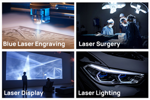 As the power of blue lasers gradually increases and the cost decreases, along with the emergence of more application scenarios, the market demand for blue lasers is unprecedentedly high. In novel applications such as blue laser engraving, medical care, display, and lighting, blue laser is drawing considerable attention from the market.
In the field of engraving and cutting, blue laser engraving devices can engrave patterns on metal, food, wood, plastic, and other materials, offering cost-effective solutions that cater to both commercial and household applications. In medical applications, blue laser surgical equipment can be used for prostate hyperplasia treatment, and its lower-power version can be used for the treatment of ear, nose, throat and digestive tract diseases. Blue laser 3D printing can be used for the production of human prostheses. The blue laser also has significant advantages in laser display applications like wide color space and long life, environmental protection, energy saving, etc., achieving the ultimate display effect, color, and clarity. In laser lighting applications, the laser lighting sources use blue laser to excite phosphors to produce white light, which can achieve higher power density and farther illumination distance and can be used in laser headlights, remote search, and many other fields.
1. Challenges in Beam Shaping of Blue Diode Lasers
Similar to near-infrared diode lasers, blue diode lasers also need to be matched with a suitable beam shaping solution in order to efficiently utilize the photon energy they emit. As an emerging field, blue laser beam shaping faces new challenges in beam shaping compared with infrared laser beam shaping:
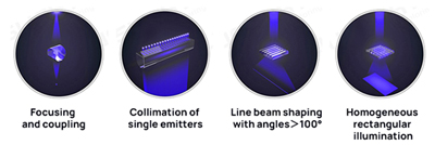 🔹The absorption rate of commonly used optical materials in the blue spectrum is higher than that in the near-infrared spectrum. Excessive absorption of laser light by materials will increase the temperature rise of optical components, causing changes in the size of optical components, thereby affecting the product performance. At the same time, the temperature rise of optical components may influence the performance and reliability of the glue that fixes the optical components, thereby affecting the optical performance and reliability of the blue laser system;
🔹Blue optics’ design needs to take into account the diverse application scenarios and packaging forms of blue lasers;
🔹There are new challenges in the coating of blue light optical components.
Depending on the applications, different beam shaping methods need to be used to meet the application's demand for photon energy.
2. Beam Shaping Solution for Blue Diode Laser
To formulate suitable beam shaping solutions for blue lasers, three aspects need to be considered: selection of optical materials, micro-optical design, and optical coating design.
a. Selection of optical materials
When selecting optical component materials for blue diode laser applications, in addition to considering parameters such as hardness and refractive index, special consideration needs to be given to the challenges posed by transmittance in the blue spectrum. Common microlens glass materials (such as S-TIH53, etc.) have good transmittance (>99.5%) for the near-infrared spectrum but have low transmittance for the blue spectrum (75%~95% for S-TIH53) and higher absorption. Excessive absorptivity can cause temperature rise and thermal lens effect, resulting in changes in the size of the microlens product, thereby affecting the optical performance of the product; the temperature rise of the micro-optical lens may also affect the performance of the glue and reduce the reliability of the system.
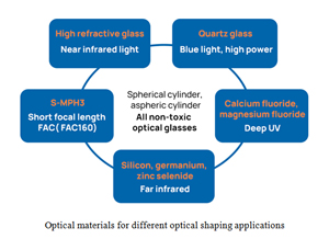 Fused silica is an ideal raw material for blue optics components. Its high transmittance (>99.5%) in the blue spectrum makes it naturally suitable for high-power blue laser applications. However, the conversion temperature of fused silica can reach 1600 degrees, which is not suitable for thermal molding or other optical processing techniques that are commonly used for aspherical lenses. Focuslight's innovative wafer-level simultaneous structuring process offers solutions to this challenge. This technique eliminates the need for heating and melting fused silica during processing. Over time, it has evolved into a mature method extensively applied in the mass production of fused silica micro-optical components. Its adoption has been widespread in recent years across various fields, including the beam shaping of infrared semiconductor lasers and UV homogenizers for photolithography machines.
On the other hand, the refractive index of fused silica is about 1.46, lower than common optical materials with a refractive index of 1.8 such as S-TIH53. This variance imposes constraints on optical design. Although optical designs such as biconvex lenses can be considered for refractive index compensation, this will significantly increase the cost and is not an ideal choice for situations where high refractive index is required. Focuslight’s wafer-level simultaneous structuring process can be used to process almost any non-toxic optical glass, including materials such as calcium fluoride, magnesium fluoride, and even silicon and germanium suitable for infrared and deep ultraviolet applications. Therefore, after two years of dedicated R&D and exploration, Focuslight has successfully developed and introduced a new material (designated as FL-Blue) that is adapted to the wafer-level simultaneous structuring process, demonstrating low absorption in the blue spectrum (transmittance >99%) and a high refractive index (n >1.7). Based on this material, Focuslight has released Blue FAC 250, Blue FAC 300, Blue FAC 380, and Blue FAC 600 series fast axis collimator (FAC) products. Additionally, small batches of blue optical components have been delivered to leading blue laser customers worldwide.
b. Micro-optical design
With the right optical materials in place, it's equally important to employ fitting optical designs that can accommodate the diverse application scenarios of blue lasers.
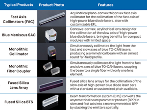 Blue diode lasers usually come in different forms such as CoS packaged single emitters, TO-can packaged single emitters, and chip arrays (bars). For different light source forms and different application scenarios, targeted designs are required to meet application needs.
At Focuslight, various micro-optical surface structures, such as aspherical cylinders, parabolas, free-form surfaces, and other surface structures can be realized using wafer-level simultaneous structuring process. Through high-precision processing of double-sided micro-optics, the integration of multiple lenses can also be achieved on micro-sized optical products.
When doing optical design, it is also necessary to consider the refraction and diffraction effects of light at the same time. Focuslight uses ray tracing algorithms and wave optics theory to conduct optical simulations, and also uses self-developed wave optics simulation software to fully simulate the diffraction effect.
 Focuslight has designed and released multiple high-performance blue laser optical component products based on different materials such as FL Blue and fused silica, such as blue fast axis collimators (FACs), blue meniscus slow axis collimators (SACs), monolithic collimators, monolithic fiber couplers, fused silica lens arrays, and fused silica beam transformation systems (BTS).
c. Optical coating design
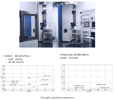
Once materials are selected and optical designs finalized, blue laser optical components undergo crucial optical coating. With over 20 years of expertise, Focuslight's team employs advanced film design and characterization techniques for complex and challenging settings, ensuring cost-effective large-scale coating production. Its coating solutions cover various types such as anti-reflection coating, high-reflection coating, ultra-low-reflection coating, filtering, and beam splitting. Customized coatings can be developed for customers based on the application requirements of different products. Focuslight also conducts tests of laser damage threshold, weak absorption, temperature rise, and environmental reliability to ensure stable, consistent performance during long-term use and mass production.
Focuslight provides a range of high-performance, high-reliability optical components for blue beam shaping. With 30 years of beam shaping excellence in micro-optical design and manufacturing, Focuslight offers precise control over photon manipulation, achieving optimal results for various applications. This expertise allows for precise photon control, ensuring ideal outcomes across diverse applications. Focuslight’s world’s leading wafer-level simultaneous structuring technology produces polished wafers up to 300 x 300 mm², offering a scalable and cost-effective solution for high-volume production, with a monthly capacity over 3 million pieces.
