New Product How the Flux H Series High-Precision Variable Laser System Drives the Advancement of Chip Packaging Technology

Semiconductor Review | Friday, August 30, 2024

As the Fourth Industrial Revolution progresses, emerging fields such as artificial intelligence, clean energy, robotics, quantum information technology, virtual reality, and biotechnology are increasingly demanding high-performance, high-precision, and high-reliability semiconductor chips and microsystems. The semiconductor chips are undergoing a rapid iteration showing four major trends:

Smaller, faster, and more energy-efficient: Advanced processing technologies and design architectures reduce chip sizes and enhance chip performance and energy efficiency.

Multi-core and heterogeneous architectures: Integrating CPU, GPU, and AI accelerators into a single chip improves multitasking capabilities and handling complex applications.

Stay ahead of the industry with exclusive feature stories on the top companies, expert insights and the latest news delivered straight to your inbox. Subscribe today.

Native artificial intelligence and machine learning: Native hardware (such as Tensor Processing Units) in the chips improves processing efficiency and enabled self-learning and adaptive capabilities.

Enhanced 2.5D/3D integration: Stacking multiple chip layers for further functions such as sensors, memory, and communication modules brings more compact and efficient chips.

These new developments impose higher demands on the semiconductor packaging process, further driving the evolution of advanced chip packaging technologies. Chip packaging provides the necessary physical protection and thermal management, directly impacting overall performance, reliability, and operability of the semiconductor chips, making it a critical role in the semiconductor manufacturing process. With the rise of System-in-Package (SiP) technology, packaging designs are becoming increasingly complex. In response, Laser-Assisted Bonding (usually abbreviated as LAB) has emerged as an innovative chip packaging technology.

LAB is an advanced micro-connection technology that leverages the high energy density of laser beams. By focusing a laser beam onto the material interface, it instantaneously heats the surface to the required temperatures, inducing physical or chemical changes in the material, resulting in a strong bond on the interface. 
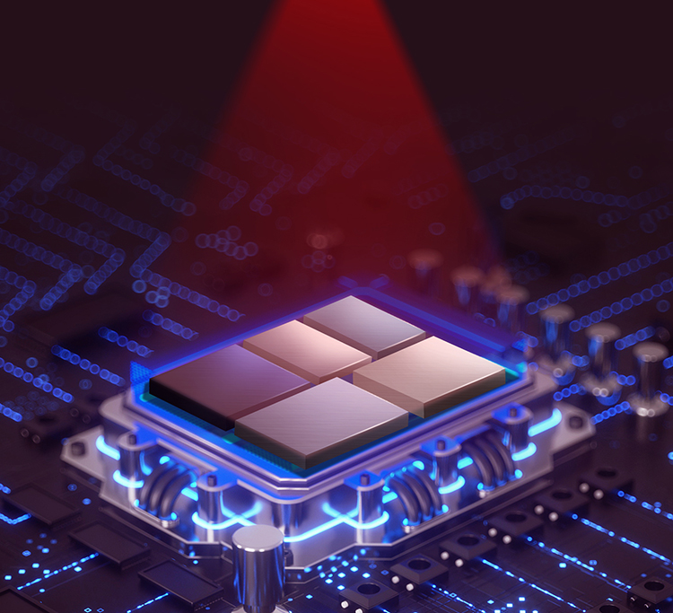
Illustration: Laser-Assisted Bonding (LAB)

LAB has been the preferred method for direct bonding of high-precision chips, offering several unique advantages in practical applications:

1. High Precision: LAB leverages the high energy density and precise control capabilities of laser beams to focus on very small areas, overcoming the limitations of traditional bonding techniques when dealing with small sizes, complex structures, or special materials. This allows for micron-level or even nanometer-level bonding precision, meeting strict requirements for bonding location and strength. Compared to traditional techniques like mass reflow or thermal compression bonding (TCB), laser-based localized heating effectively prevents yield reduction caused by thermal expansion without requiring additional measures.

2. Non-Contact: Unlike traditional mechanical bonding or thermos-compression bonding, LAB is a non-contact bonding method. The laser beam heats and melts the material surface, achieving bonding without mechanical damage or contamination, thereby improving the quality and reliability of the bond. This makes LAB particularly suitable for bonding fragile materials and miniature devices.

3. High Speed: LAB enables rapid bonding with the laser energy being instantly transmitted to the bonding interface. Bonding time can be reduced to just a few milliseconds or even less, significantly improving production efficiency, making it ideal for mass production and high-output electronics manufacturing.

4. Versatile: LAB can accommodate bonding requirements for various materials, including metals, semiconductors, ceramics, and glass, offering broad application prospects in the electronics packaging applications.

5. Scalable: LAB can be combined with other packaging techniques, such as flip-chip and wafer-level packaging, to achieve more complex electronic packaging structures.

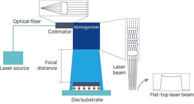
To ensure the quality and reliability, the LAB process requires precise control of key output specifications such as laser energy, uniformity, wavelength, and exposure time. Typically, an LAB system should include the following major parts to achieve the goal:

1. High-Power Semiconductor Laser Source: Generates continuous output laser energy at a wavelength of 980nm.

2. Optical Fiber: Transmits laser energy from the source to the optical shaping modules.

3. Collimation Module: Collimates the laser beam to increase its directionality and focusing capability.

4. Adjustable Homogenization Module: Produces a flat-top laser beam with adjustable width and length, ensuring uniform power density distribution across the beam. This ensures homogeneous heating of the bonding components, avoiding temperature inconsistencies caused by power distribution.

5. Synchronous Temperature Control Unit: Monitors the temperature of the process area in real-time and controls the laser output in a closed-loop manner to ensure process consistency and stability.
On August 28, 2024, Focuslight officially launched the Flux H Series High-Precision Variable Laser System for Advanced Chip Packaging Processes, which offers the following features and advantages:

1. Independently Adjustable Beam Size: Adaptable to requirements of different packaging structures with flexible processing solutions.

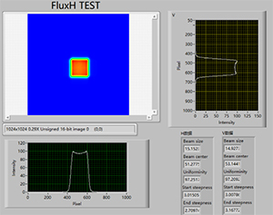
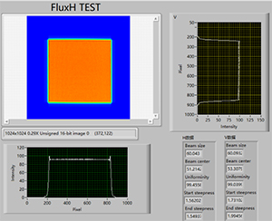
2. High Beam Uniformity: A high uniformity standard of ≥ 95% across the entire beam area ensures bonding quality and process stability. No hot-spots in the beam that could reduce the process yield.

3. Large Depth of Focus: Suitable for packaging processes involving multilayer and complex structures. This provides greater flexibility in handling different packaging heights and complexities.

4. High-Accuracy Beam Center: within the beam adjustment range, the system ensures high-precision beam positioning during the bonding, which is crucial for the packaging process requiring precise heat input control.

5. Excellent Steepness at Beam Edge: A typical beam edge steepness of ≤ 3mm maintains a high energy concentration even at the edges of the processing area. It also effectively prevents overheating and reduces the thermal impact on sensitive surrounding areas.
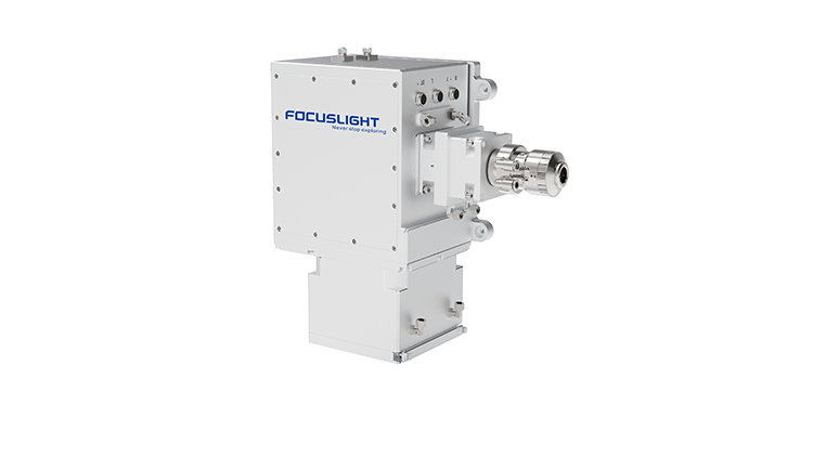
Flux H Series High-Precision Variable Laser System for Advanced Chip Packaging Processes

Key Specifications and Typical Test Results: 

Item

Unit

Typical Value

CW-nominal Output Power

W

6000

Wavelength

nm

976 ± 10

Working Distance

mm

480 ± 10

Focal Depth

mm

≥ ± 1

Line Length X-direction (top-hat)

mm

15 – 60

Line Length Y-direction (top-hat)

mm

15 – 60

Beam adjustment method

/

Continuous independent adjustable

Uniformity of X and Y-direction

/

≥ 95%

Beam center position deviation

mm

≤ ± 0.3

Steepness of X and Y-direction

mm

≤ 3

The optical efficiency

/

≥ 88%

Focuslight’s newly launched Flux H Series High-Precision Variable Laser System offers highly efficient and reliable solutions for advanced chip packaging processes with its superior performance and versatile applications. The typical configuration of Flux H Series is now available for customer orders with customization possibilities aligning with customer needs. Through innovation, manufacturing excellence, and fast response, Focuslight remains committed to be your globally trusted partner in the photonics industry.


More in News

Silicon wafer suppliers occupy a critical position in modern technology, powering innovation across electronics, renewable energy, automotive, and communication systems. Their evolution mirrors continuous advancements in precision engineering, efficiency, and sustainability. Through ongoing improvements in wafer design and production processes, suppliers enable industries to achieve higher performance, reduced costs, and scalable reliability. These innovations form the backbone of global technological progress, driving growth and shaping the future of multiple sectors. Precision Manufacturing and Innovation Continuous improvement in wafer quality has become a defining trend in the industry. Suppliers have invested in advanced polishing, slicing, and refinement methods that reduce defects and deliver ultra-flat surfaces. Such precision allows manufacturers to integrate wafers into increasingly complex devices, from microprocessors to high-power sensors, with maximum efficiency. Larger wafer sizes are also gaining prominence, providing economies of scale that improve chip output and reduce production costs for global industries. Surface engineering has introduced breakthroughs in stress management and heat resistance. By incorporating ultra-thin protective coatings and innovative treatments, suppliers are producing wafers that can withstand intense thermal and electrical loads. These improvements ensure reliability for high-performance applications such as artificial intelligence, autonomous vehicles, and medical technologies. Tailored manufacturing approaches now offer flexibility in wafer specifications, meeting the diverse needs of clients developing next-generation devices. Digitalization further enhances production efficiency. Automated systems and real-time monitoring enable suppliers to reduce variability, strengthen quality control, and streamline their operations. These innovations increase consistency while ensuring that wafers meet the rigorous standards of advanced applications. Sustainability and Market Growth Opportunities Sustainability has become a central focus in the production of silicon wafers. Recycling silicon waste and adopting energy-efficient processes reduces the environmental footprint while ensuring a consistent supply of raw materials. Closed-loop production methods are gaining traction, allowing suppliers to reclaim and repurpose silicon without compromising quality. These practices align with global demands for environmentally responsible manufacturing. Expanding demand across sectors such as renewable energy, smart devices, and electric vehicles presents significant growth opportunities. Solar energy applications, in particular, are driving the need for high-quality wafers that enhance efficiency and durability. Suppliers are responding by refining technologies that maximize energy output while lowering production costs, reinforcing their role in advancing sustainable solutions. Globalization also fuels opportunities in cross-border collaborations. Suppliers capable of navigating diverse market regulations and customer requirements strengthen their competitiveness in an interconnected economy. Personalized wafer solutions provide a competitive edge, enabling suppliers to deliver innovations tailored to unique industrial applications while fostering stronger partnerships. ...Read more
Semiconductor chip manufacturing is the backbone of today’s digital world. These tiny components power everything from personal electronics to national infrastructure. As technology evolves, the precision and scale of chip production become even more crucial, driving innovation, economic growth, and global security in an increasingly connected and competitive landscape. The Foundation of Modern Technology Semiconductor chips are at the core of nearly every modern electronic device. These tiny components enable complex operations, from smartphones and computers to cars and household appliances. Their role is not just limited to consumer electronics. They are integral to telecommunications, healthcare devices, industrial machinery, and defense systems. Chip manufacturing is essential because it keeps these critical sectors functioning smoothly. The increasing complexity of digital technologies requires chips with higher performance and energy efficiency. Manufacturing these chips is not a simple process. It involves intricate steps carried out in highly controlled environments. Even a speck of dust can ruin an entire batch. The precision and sophistication required in this industry mean that the knowledge, infrastructure, and talent involved must operate at the highest standards. Reliable chip production ensures consistent innovation and seamless operation across countless industries. Without a steady supply of semiconductor chips, entire technological ecosystems can come to a standstill. Lapses in availability directly affect the production of electronic goods, impacting businesses, economies, and daily life. Economic and Strategic Significance Beyond technology, semiconductor chip manufacturing is critical in shaping national economies and global competitiveness. Countries with strong manufacturing capabilities gain a potent edge in economic growth, job creation, and industrial development. This sector fuels a wide supply chain, supporting industries that range from chemical processing to software development. High demand for advanced chips has focused intensely on self-sufficiency and domestic production capabilities. Governments and industries increasingly see chip manufacturing as a national security priority. The ability to produce chips independently can protect nations from supply disruptions, geopolitical tensions, and over-reliance on external sources. It ensures that critical infrastructure, such as power grids and communication networks, remains operational under all conditions. Investments in this field also drive research and development, further contributing to materials science, nanotechnology, and engineering innovation. These advancements often trickle down into other sectors, spurring broader technological progress. The workforce employed in chip fabrication includes highly skilled engineers, scientists, and technicians. Their expertise is vital for producing current generations of chips and developing the next wave of technologies. ...Read more
The global capacitor market is experiencing steady growth, and capacitor solutions providers are becoming vital enablers of performance, energy efficiency, and innovation in modern electronics. Several market factors contribute to this increasing demand. Capacitors, essential for energy storage, filtering, and voltage regulation, are embedded in nearly every electronic device, from smartphones and laptops to automotive powertrains and medical equipment. The widespread application requires highly reliable, compact, and temperature-resilient capacitor solutions. Providers are integrating newer dielectric materials, including ceramic, tantalum, aluminum, and film-based technologies, to offer capacitors with higher capacitance, lower equivalent series resistance (ESR), and greater operational stability under harsh conditions. Innovations in nanotechnology and material science are leading to the development of ultra-miniaturized capacitors, enabling the production of thinner and more powerful electronic devices. The adoption of surface-mount technology (SMT) and multilayer ceramic capacitors (MLCCs) has gained momentum due to their ability to deliver enhanced electrical properties in compact formats. Impact of Digital Innovation and Sustainability The emergence of digital twins, automated manufacturing, and AI-enabled quality control systems is redefining production practices. Capacitor providers now employ advanced simulation tools to model capacitor performance under different environmental conditions, helping in predictive failure analysis and reliability enhancement. Automated production lines ensure uniformity and scalability, while smart sensors and AI-driven inspection systems detect microscopic defects, minimizing product failure rates. The technologies reduce costs and defects and shorten the time-to-market for custom capacitor solutions, a critical competitive edge in sectors like automotive and aerospace. Capacitor providers are responding with high-voltage, long-life capacitors that support regenerative braking, onboard charging, and power electronics in hybrid and electric drivetrains. Another trend is the increasing use of polymer-based capacitors, which offer high ripple current capabilities and enhanced safety for automotive and telecom applications. Strategic Value Across Industries Capacitor solutions providers are critical partners across multiple industries by enabling various electronic systems' functionality, stability, and efficiency. In consumer electronics, capacitors support power management, energy buffering, and noise suppression in devices like smartphones, wearables, gaming consoles, and smart TVs. As devices become slimmer and more feature-packed, the demand for high-capacitance, miniaturized components grows. Providers offer MLCCs and thin-film capacitors with optimized size-to-performance ratios that meet these design requirements while ensuring product reliability. In the automotive sector, capacitors play a crucial role in infotainment systems, advanced driver-assistance systems (ADAS), lighting, and battery management. High-temperature and high-voltage capacitors are essential for DC/DC converters, inverters, and electric powertrains, particularly in EVs and hybrid vehicles. Capacitor providers deliver solutions that offer thermal stability, high ripple current tolerance, and extended life under vibration and stress. These characteristics help maintain the safety and performance of EV systems, reduce energy losses, and improve battery longevity. Capacitors in energy storage systems also support frequency regulation and peak shaving, making them critical to grid stability and load balancing. Custom film and power capacitors with self-healing properties and long operational lifespans are highly sought after. Healthcare and telecommunications also rely heavily on capacitors for equipment stability and data transmission. Capacitors maintain a consistent power supply in base stations and fiber-optic networks for telecom infrastructure, preventing signal degradation and downtime. With the rollout of 5G and the proliferation of edge computing, capacitor providers must meet tighter size constraints, higher frequencies, and increased reliability standards. Capacitor solutions also extend to aerospace and defense, where performance under extreme environments is critical. Providers supply radiation-hardened, ruggedized capacitors that operate under extreme temperatures, shock, and vibration. These are used in satellites, radar, avionics, and mission-critical control systems. Capacitor solutions providers help safeguard national defense and space exploration efforts by ensuring electronic integrity in high-stakes applications. Ethical Sourcing in Capacitor Production: Innovations and Diversification Capacitor providers are diversifying supply sources, investing in material recycling, and developing alternative compositions that reduce dependency on conflict materials. It is particularly challenging in high-power applications where heat dissipation and long-term stability are critical. Providers are investing in advanced materials, such as high-k dielectrics and nano-coatings, to boost capacitance without increasing size. Cloud-based design tools and simulation software help optimize product development cycles, enabling quicker turnaround for customer-specific solutions. They adopt modular designs that allow stacking or combining capacitor types for hybrid performance in compact packages. The rise of smart cities, autonomous vehicles, wearable medical devices, and IoT ecosystems will require increasingly specialized energy-efficient, miniaturized, and highly reliable capacitors. Capacitor providers must evolve alongside these industries, offering components and complete engineering support, simulation tools, and life-cycle services. Sustainability will also play a greater role in product development and business strategy. Providers will face increasing pressure to adopt circular economy principles, minimize hazardous substances, and reduce the carbon footprint of manufacturing processes. The shift toward biodegradable capacitors, recyclable packaging, and energy-efficient production lines is underway and expected to accelerate in the coming years. Capacitor solutions providers occupy a pivotal space in the global electronics landscape, enabling innovation across multiple industries through advanced design, reliable performance, and continuous adaptation. Their strategic importance will only increase in the age of electrification, digitization, and intelligent systems, making them critical contributors to the world’s technological progress. ...Read more
 The semiconductor industry is evolving to meet modern demands, with printed electronics poised to revolutionize both manufacturing and performance. Unlike traditional silicon-based semiconductors, which involve complex and resource-intensive fabrication, printed electronics offer a more cost-effective and flexible solution. This technology uses conductive inks and advanced printing methods, such as screen printing and inkjet printing, to create components like transistors, sensors, and even entire circuits on flexible materials. It is especially beneficial in the semiconductor industry, where there is an increasing need for smaller, lighter, and more efficient devices. Printed electronics pave the way for innovations that can result in more compact designs and enhanced functionality while maintaining high performance. One of the most notable advancements in printed electronics within the semiconductor sector is the ability to produce high-performance devices without the constraints of traditional manufacturing methods. The development of novel conductive inks, which exhibit excellent electrical properties, has enabled the fabrication of high-frequency circuits suitable for RF applications. These advancements make it possible to produce semiconductors operating at lower power levels while maintaining high-speed performance. The flexibility of printed electronics allows for the easy integration of various components into a single substrate. This integration can lead to the development of multifunctional devices that combine sensors, transistors, and antennas, all within a single printed layer. This seamless integration is particularly beneficial for applications in the Internet of Things (IoT), where compactness and connectivity are paramount. Another significant advantage of printed electronics in the semiconductor industry is sustainability. Traditional semiconductor manufacturing processes involve significant waste and high energy consumption. In contrast, printed electronics utilize fewer raw materials and create less waste, making them a more environmentally friendly option. Additionally, the cost-effectiveness of printed electronics is enticing for manufacturers; the roll-to-roll printing technique allows for mass production of electronic components, reducing the cost per unit significantly. These characteristics make printed electronics a viable alternative, especially considering the increasing costs associated with traditional semiconductor production. As technology advances, the potential applications of printed electronics within the semiconductor industry are immense and continually expanding. Flexible and wearable electronics, smart packaging, and advanced medical devices are just a few areas in which to benefit from these advancements. For instance, in the medical field, printed flexible sensors can be embedded in wearable devices for continuous health monitoring, providing real-time data without bulky traditional electronics. Partnerships between semiconductor companies and research institutions are critical to advancing printed electronics technology. By collaborating and sharing expertise, the industry can speed up the development of new materials, inks, and printing techniques that will enhance performance and expand the applications of printed electronics. ...Read more