


The long-term development logic of the LED industry aligns with "Haitz's Law", which is the continuous improvement of luminous efficiency and cost reduction. These two factors together drive the penetration of LED applications and technological advancements, analogous to the semiconductor Moore's Law - the LED industry experiences a 20-fold increase in production output every decade, while costs have decreased to one-tenth of their original value. Over the past 30 years, high power, miniaturization, and full-color capabilities have emerged as key drivers for LED applications in the fields of displays, backlighting, and lighting.
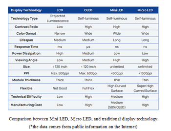 Mini LED and Micro LED (also known as μLED) refer to LEDs with chip sizes smaller than 200μm and 50μm, respectively. Same as conventional LEDs, they are self-emissive and typically used in direct display applications of varying sizes, where each pixel can be individually controlled using RGB LED chips that emit three different colors of light. From a technical and display standpoint, Mini and Micro LEDs inherit the characteristics of LEDs. With energy consumption of only 10% of LCD and 50% of OLED, they offer 30 times the brightness of OLED and a resolution of up to 1500 PPI. In addition to these advantages, they also exhibit high reliability, fast response times, long lifespans, and quick refresh rates.
Stay ahead of the industry with exclusive feature stories on the top companies, expert insights and the latest news delivered straight to your inbox. Subscribe today.
Over the next decade, as LED chips continue to decrease in size and cost and manufacturing challenges being overcome. There is a projection that the Mini and Micro LED will bring about a revolution in backlighting and display technologies. These advancements have the potential to become the ultimate solution for various applications, including commercial displays, wearable devices, smartphones, computers, and more.
The development of new technologies will inevitably bring about continuous iteration and upgrading of process technologies. In the process of developing from Mini LED to Micro LED, as the size of a single LED chip is reduced by multiples, its display effect and precision have been improved, and the number of LED chips used in the same area has also increased by multiples. Taking the 4K resolution direct display panel as an example, it has nearly 8.3 million display pixels and about 24 million LED chips. Due to the need for such a huge amount of chips, mass transfer, mass soldering, chip repair, and drive control technology in the panel manufacturing process now require new groundbreaking processes to solve technical problems.
1. Laser Mass Transfer
In the field of Mini and Micro LED display technology, the primary challenge to address lies in the mass transfer of chips. This complex transfer typically involves multiple pivotal steps: the collective release of Micro LED chips from the donor/growth substrate, the adjustment of chip pitches, and the precise alignment and movement of chips onto the receiving substrate. The conventional mechanical transfer equipment can only transfer tens of chips per second, which falls short of meeting the demands for large-scale production of Micro LEDs. Consequently, mass transfer technology has emerged to overcome this limitation.
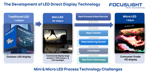 Commonly used chip mass transfer methods include Electrostatic Adhesion Transfer, Fluid Assembly Transfer, Elastic Impression Transfer, Laser Mass Transfer, etc.
Through continuous technological development and iteration, mass transfer is considered a highly beneficial and efficient solution. Its principle involves the interaction between materials and laser beams generated by laser devices, wherein the LED substrate material absorbs photons of ultraviolet (UV) wavelength, leading to a change in its properties. As a result, a large number of LED chips can be simultaneously detached from the substrate. This transfer technique requires precise control of the laser power and energy density to ensure minimal impact on the chip performance and achieve high transfer yield and efficiency.
 Focuslight offers comprehensive photon application solutions for Mini LED and Micro LED’s mass transfer, utilizing its core technologies in photon generation and photon control. Based on the laser light source in the ultraviolet (UV) band, Focuslight leverages ultraviolet (UV) wavelength laser sources to design flexible optical solutions that cater to the varying process requirements of our customers. These solutions are tailored to achieve customized laser beam -features for the mass transfer process, ensuring a comprehensive balance between laser power, energy uniformity, and beam size. This enables us to match the mass production needs and capacity requirements of customers with different product sizes.
2. Laser Mass Soldering
Mass soldering is another critical step in the main manufacturing process of Mini and Micro LED displays. The traditional soldering method uses a reflow oven to join the LED chips and electrodes together by melting and solidifying the solder. The solder solidification process goes through a solid-liquid-solid phase transition. However, due to the small size of the LED chip, displacement can arise during the crystallization process. Moreover, the prolonged heating process within the reflow oven, which necessitates heating the entire substrate, can lead to substrate deformation issues during the reflow.
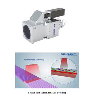 As an alternative technology to the traditional method, laser mass soldering has the advantages of short heating time, controllable soldering effect, no significant displacement of the chip, selectable heating area, and no deformation of the substrate. However, laser reflow soldering with traditional "point-shape" light sources has been greatly challenged in this application. Taking a 4K Micro LED TV as an example, the number of pixels are 4096×2160 (about 8.3 million pixels) and each pixel has an RGB three-color chip, then the total number of chips is about 24 million. When it comes to point beam soldering, the productivity is incredibly low, making it difficult to achieve the desired results. Therefore, laser “mass soldering” becomes the optimal solution.
Mass soldering refers to the process of simultaneously soldering multiple LED chips within a specific area, which is in a good contrast to the traditional soldering methods that can only handle one point at a time. Implementing Focuslight's innovative photon control technology, mass soldering can transform the conventional point-shape beam into a homogeneous and extended area beam that is employed to heat simultaneously larger soldering areas of Mini and Micro LED chips. Through the process, the LED chips are heated and soldered all at once, resulting in the desired productivity of mass soldering.
3. Laser Chip Repair
To enhance the yield rate of the mass transfer and mass soldering for Mini LED and Micro LED chips, spatially defined repairing of LED pixel becomes a crucial step in the process. For instance, the mass transfer process must maintain an accuracy of within plus or minus 0.5 microns for each chip to ensure the yield, but even with a yield rate as high as 99.999%, a 4K TV will still have approximately 260 dead pixels that require repair. This is where the laser's high precision and directivity play a significant role. Typically, the laser chip repair process involves several steps such as AOI (Automated Optical Inspection) detection, laser removal, and laser soldering. Initially, high-precision detection equipment is utilized to identify and locate dead spots on the chips. Subsequently, high-peak energy laser beams are employed to remove these dead spots. Finally, the single chips undergo transfer and laser soldering repair, ultimately completing the repair process for the dead spots.
Focuslight provides comprehensive photon application solutions for Mini LED and Micro LED chip repair powered by our own core technologies of photon generation and photon control. A good example is our NIR laser systems with extremely small rectangular beam output, where the beam size can be customized according to the target applications: The minimum beam length can reach as short as 50μm, while the energy output in the length and width direction can still be top-hat with a uniformity of >97%, making it an optimal solution to the repair of LED chips in different sizes.
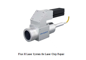 Focuslight was an early pioneer in recognizing the emerging growth potential of Mini & Micro LED technology. Since 2019, the company has been at the forefront of research and development in the field of mass soldering for Mini & Micro LEDs. Over the past two years, Focuslight has successfully collaborated with various customers in the laser mass transfer and laser chip repair sectors, leveraging its extensive know-how in diode lasers and beam shaping technologies. Through years of dedicated research and accumulation of expertise, Focuslight proudly introduced the Flux H series laser system. This product is designed to offer efficient photon application solutions specifically tailored to laser mass soldering and laser chip repair.
The Flux H laser system (designed for mass soldering applications), utilizes a fiber-coupled diode laser source operating at a wavelength of 976nm and delivering a power ranging from 4000 to 10000W. Powered by Focuslight’s proprietary optical design, the Flux H regulates the beam size and homogenization through micro-optic modules from both the beam length and width directions. The output beam is continuously adjustable in its width and length from 2mm to 200mm, as the uniformity maintains as high as > 97%.
The Flux H laser system (applied to laser chip repair ) uses a fiber-coupled diode laser source with a power of 30-150W and a wavelength of 976nm. The length and width of the output beam can achieve precise size control (365µmx105µm) and excellent optical homogenization with a uniformity exceeding 90 %.
Focuslight’s Flux H series laser system masters the following three key points of Mini LED and Micro LED mass soldering and laser chip repair process, and provides optimal solutions.
Beam control: Focuslight’s unique Refractive Optical Elements (ROE) shaping technology enables diode lasers to output large or precisely small beam spots in square, linear, and rectangular geometries. Customers can choose the standard beam size or customize the beam parameters according to their specific needs. This allows for one-time soldering of the entire area covered by the beam, truly achieving the goal of massive soldering and precise laser chip repair through accurately sized spots.
Uniformity: Thanks to Focuslight’s homogenization technology, the upper limit of the beam uniformity can reach 99% with no zero-order diffraction. In actual products, the beam uniformity can be as high as >97%, effectively ensuring high yields and outstanding consistency within the soldering area.
Closed-loop temperature control: The closed-loop temperature control can effectively simulate the control process of the high-temperature reflow oven. It enables the editing of temperature-time envelopes and the realization of processes such as solder paste preheating > heat up > heat preservation > cool down > cooling.
As an industry leader in high-power diode laser and its application solutions, is capable of providing tailored photonics application solutions for Mini and Micro LED display processes, covering components, modules, assemblies, and subsystems. Focuslight strives to be the globally trusted photonics solution provider through innovation, manufacturing excellence, and fast response to fully unlock the potential of photonics to enhance and enrich people's life!
 About the Author:
Weiyi Gu, Vice President of Focuslight’s Pan-Semiconductor Solutions Business Unit. Graduated from the School of Telecommunications of Xi’an Technological University with a master's degree in engineering. He has more than ten years of experience in the field of laser applications and focuses on the product and application development of high-power diode laser systems in advanced manufacturing and pan-semiconductor fields. He has led the development of Focuslight’s DLight H, DLight S, and Flux H series high-power diode laser systems.
