


Thank you for Subscribing to Semiconductor Review Weekly Brief
× 
Semi Conductor Review Weekly Brief
Be first to read the latest tech news, Industry Leader's Insights, and CIO interviews of medium and large enterprises exclusively from Semi Conductor Review
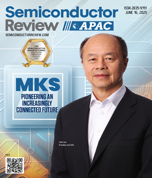
MKS has been recognized by Semiconductor Review Magazine as “Top Semiconductor Manufacturing Solutions Provider In Apac 2025” based on our proprietary methodology, reflecting its position in the industry. This profile has been developed by the Semiconductor Review research and editorial team based on insights from an interview with John Lee, President and CEO.


 John Lee, President and CEO
To counter this slowdown, the semiconductor industry is strategically pivoting towards heterogeneous integration and advanced packaging. This paradigm shift moves beyond encapsulating a single chip to integrating multiple specialized dies into a unified package that operates as a cohesive system. It offers a modular approach to increasing input/output density and sustaining performance gains in electronic devices, effectively extending the trajectory of progress beyond the limitations of traditional scaling–a concept often dubbed "More than Moore's Law." This technology is no longer niche; it is becoming indispensable across a vast spectrum of microelectronics applications, from the power-hungry AI and HPC servers demanding colossal processing power and high-bandwidth memory to the size, weight, and power-conscious requirements of mobile devices. The diverse and evolving demands of these applications are continuously propelling the innovation and refinement of advanced packaging architectures and process technologies.
This transition is not without its challenges. The increasing complexity of advanced packages, driven by the demands of AI, renewable energy systems, autonomous vehicles, and other high-performance applications, presents significant hurdles in manufacturing spanning several critical areas.
• Larger package sizes and increased I/O density: The insatiable appetite of AI and HPC for computational power and memory bandwidth necessitates larger package sizes to accommodate a greater number of HBM stacks. This trend, coupled with the move towards 3D heterogeneous integration on interposer combined with a package substrate, demands innovative materials and processes capable of handling increased complexity and stringent performance requirements.
• Shrinking feature sizes and interconnect pitch: Next-generation chip designs rely on increasingly higher I/O densities, pushing the boundaries of interconnect technology and requiring significantly smaller pitches. Micro bumps are reaching their limitations, necessitating the exploration and adoption of advanced interconnect solutions like Cu-Cu hybrid bonding.
• Reliability and contamination control: As packages become more complex with finer features and multiple integrated dies, ensuring long-term reliability and stringent contamination control throughout manufacturing becomes paramount. This is particularly critical for demanding applications like automotive and aerospace.
• Thermal management: The increasing power density within advanced packages, driven by the integration of more dies and passive components, poses a significant thermal management challenge. Efficiently dissipating the generated heat is crucial for maintaining performance and reliability.
• Material compatibility and warpage: Integrating diverse materials with varying thermal and mechanical properties in advanced packages can lead to issues like warpage, especially with larger substrate sizes. This necessitates the exploration of new substrate materials such as glass, which offer superior thermal stability but require novel processing techniques.
-
Our investments are important milestones as we expand our leadership across and beyond semiconductor manufacturing to meet the skyrocketing demand for AI and HPC server chips
• Material compatibility and warpage: Integrating diverse materials with varying thermal and mechanical properties in advanced packages can lead to issues like warpage, especially with larger substrate sizes. This necessitates the exploration of new substrate materials such as glass, which offer superior thermal stability but require novel processing techniques.
• Energy efficiency and sustainability: The exponential growth of AI and data centers is driving tremendous energy demands. Enhancing energy efficiency at every level – from the chip design to the manufacturing process – and adopting sustainable manufacturing practices are becoming increasingly critical.
• Design complexity and tooling: Designing and optimizing complex 3D heterogeneous packages requires sophisticated tools and methodologies that can handle multi-physics domains. The current disconnect between chip-level and package-level design kits adds to this complexity.
• Manufacturing cost and yield: Achieving cost-effective manufacturing with high yields for these complex advanced packages remains a significant challenge. This requires continuous innovation in materials, equipment, and processes.
 Future challenges and potential solutions:
Looking ahead, the demands on semiconductor manufacturing will only intensify. The continued evolution of AI, the proliferation of the Internet of Things, and the advancements in autonomous systems will push the boundaries of performance, power efficiency, and miniaturization even further. Some key future challenges and potential solutions include:
• Beyond Moore's Law scaling: As traditional scaling reaches its physical limits, the industry will need to rely even more heavily on innovative packaging technologies, new materials, and novel device architectures to achieve performance gains. Optimizing the entire system from chip design to packaging, will become crucial.
• Hybrid bonding: This technology holds immense promise for achieving higher-density connections, increased bandwidth, and improved energy efficiency by directly bonding chip surfaces. Overcoming challenges in overlay optimization and achieving tight process control, akin to front-end wafer processing, will be key to its widespread adoption.
• Photonics integration: Integrating photonics with electronics within and between packages offers the potential for significantly higher bandwidth and energy efficiency for data transfer. Continued investment in R&D is needed to demonstrate feasibility and optimize energy consumption in laser systems.
• Advanced substrate materials: Adopting new substrate materials like glass panels, with their superior thermal stability and potential for denser interconnects and double-sided processing, will require the development of new inspection, metrology, and processing techniques.
• Integrated design and manufacturing: Merging chip-level and package-level design kits will enable superior designs and more efficient manufacturing processes. This requires greater collaboration between design companies, materials suppliers, and equipment manufacturers.
• Advanced thermal management solutions: Innovations in materials with high thermal conductivity, such as Aluminum Nitride, and integrating efficient cooling solutions within packages will be critical to address the increasing heat densities. Silicon Carbide power devices can also improve energy efficiency and thermal management at the system level.
• Sustainable manufacturing practices: The industry will need to prioritize the development and adoption of more environmentally friendly manufacturing processes, including reducing waste, conserving energy, and utilizing sustainable materials.
Strategically Positioned to Address the Demand
MKS is strategically positioned as a critical enabler in semiconductor manufacturing, particularly in advanced packaging. With broadened capabilities from targeted acquisitions and a commitment to innovation, MKS delivers comprehensive solutions that help customers meet the evolving complexities of next-generation microelectronics.
The acquisitions of Electro Scientific Industries (ESI) in 2019 and Atotech in 2022 have significantly strengthened MKS’s capabilities in interconnect process technologies. ESI’s leadership in laser via drilling and Atotech’s expertise in specialized chemistries support MKS’s Optimize the InterconnectSM offering—an integrated solution that accelerates time-to-market for advanced packaging applications, including larger HBM stack capacities, 3D heterogeneous integration, and AI/HPC-driven substrate and MLB/hybrid board designs.
Atotech also expanded MKS’s portfolio into advanced plating equipment and software solutions. Recent investments at APAC technology centers, including the G-Plate® (a next-generation HVM PTH tool for <5/5 µm lines and spaces) and Geode™ A (a high-precision CO₂ laser system for ABF laminate processing), enable faster development cycles for high-end SAP technologies—addressing the needs of AI, HPC, automotive, and industrial IoT applications.
MKS offers a unique one-stop-shop for optimized laser drilling, plating, surface modification, and final finishing—delivering higher yields, faster production cycles, and superior performance without production interruption.
"These investments are important milestones as we expand our leadership across and beyond semiconductor manufacturing to meet the skyrocketing demand for AI and HPC server chips," says John Lee, President and CEO of MKS Inc..
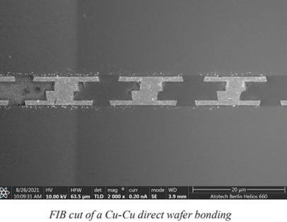
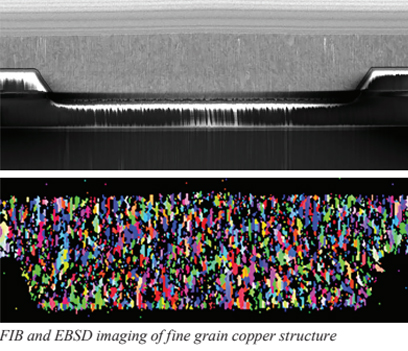 MKS’s commitment to tackling leading-edge design challenges is evident in its advanced plating portfolio. The Atotech Everplate® Cu series meets the stringent demands of Cu-Cu hybrid bonding, delivering copper deposits with a metastable microstructure that recrystallizes during bonding to form a highly reliable Cu-Cu interface. Its ability to efficiently fill fine bonding structures with excellent process stability enables higher I/O densities, superior electrical performance, and reduced device footprint. As pitch sizes shrink, Cu-Cu hybrid bonding offers clear advantages over traditional soldering, including smaller form factors, enhanced reliability, and better overall performance.
In barrier plating, Spherolyte® NiFe enhances reliability by reducing intermetallic compound (IMC) growth through iron co-deposition in the nickel diffusion layer—minimizing solder depot consumption and boosting micro bump durability.
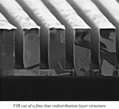
MKS’s market-proven solutions, like Spherolyte® Cu UF3, are engineered for fine-line Redistribution Layer (RDL) plating, delivering extremely pure copper deposits, exceptional voiding performance, low resistivity, and deployment versatility across various plating platforms. This addresses the critical need for high-purity, low-stress, and highly reliable copper structures in next-generation semiconductor advanced packaging.
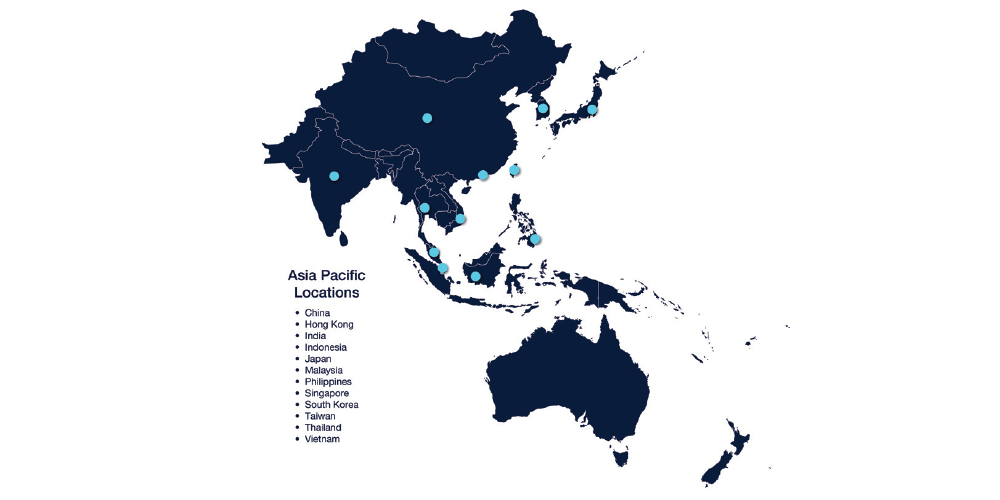
Recognizing the growing importance of the APAC region, MKS has established a strong and industry-leading presence with sophisticated equipment, process know-how, and highly skilled expert teams. With 14 manufacturing facilities in Asia alone, including significant investments in new Supercenters in Penang, Malaysia, and new facilities in Thailand, MKS is strategically expanding its capacity to meet the skyrocketing demand for AI, HPC, automotive technologies, and IIoT solutions.
 At the Forefront of Semiconductor and Advanced Packaging Innovation
The semiconductor and advanced packaging manufacturing landscape is undergoing a profound transformation, driven by the insatiable demands of emerging technologies like AI and HPC. While significant challenges exist in areas such as package complexity, shrinking feature sizes, thermal management, and sustainability, the industry is actively pursuing innovative solutions such as advanced packaging, hybrid bonding, new substrate materials, and integrated design flows. MKS, with its strategic acquisitions, comprehensive portfolio of technologies, deep process expertise, and expanding global presence, is exceptionally well-positioned to support its customers in navigating these challenges and capitalizing on the opportunities of this dynamic and critical industry. By providing superior end-to-end solutions and proactively addressing the evolving needs of advanced electronics manufacturing, MKS is a key enabler in shaping our increasingly connected future.
| Share this Article:Tweet
|
Company
MKS
Management
John Lee, President and CEO
Description
MKS develops leading process and manufacturing technologies for advanced surface modification, electroless and electrolytic plating, and surface finishing. Applying a comprehensive systems-and-solutions approach, the Atotech portfolio includes chemistry, equipment, software, and services for innovative and high-technology applications. These solutions are used in a wide variety of end-markets, including data center, consumer electronics and communications infrastructure, as well as in numerous industrial and consumer applications such as automotive, heavy machinery, and household appliances.
This content is copyright protected
However, if you would like to share the information in this article, you may use the link below: