
Thank you for Subscribing to Semiconductor Review Weekly Brief
× 
Semi Conductor Review Weekly Brief
Be first to read the latest tech news, Industry Leader's Insights, and CIO interviews of medium and large enterprises exclusively from Semi Conductor Review
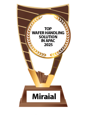
Miraial has been recognized by Semiconductor Review Magazine as “Top Wafer Handling Solution in APAC 2025” based on our proprietary methodology, reflecting its position in the industry. This profile has been developed by the Semiconductor Review research and editorial team based on insights from an interview with Masatoshi Hyobu, President.



Miraial
Advanced Wafer Handling for High-Tech Semiconductor Manufacturing

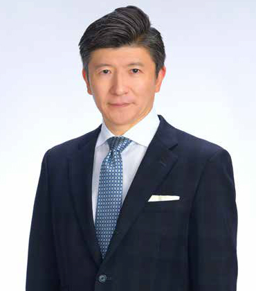 Masatoshi Hyobu, President
With the industry’s rapid shift toward automation, high-quality and high-volume manufacturing, semiconductor fabs require handling solutions that align with evolving manufacturing processes. Miraial works directly with device makers to understand their requirements and develop precision-engineered wafer-handling systems.
Its front-opening unified pods (FOUP), front-opening shipping boxes (FOSB) and wafer cassettes protect wafers from contamination and mechanical stress throughout their handling process. Tailoring these products to specific wafer sizes, thicknesses, and material compositions enhances production reliability and contamination control. These precisely engineered solutions integrate seamlessly into next-generation fabrication processes and enable fabs to maintain the most rigorous cleanliness and quality control standards.
“As a customer-centric company, we highly value customer feedback, which is integral to our product development and quality improvement,” says Takamasa Kato, executive director.
The rising demand for advanced, high-performance chips pushes semiconductor companies to refine their material handling processes, requiring more sophisticated solutions. Governments and industry leaders worldwide are strengthening domestic semiconductor capabilities. As companies restructure supply chains to meet evolving demands, Miraial’s customer base is shifting, driving demand for innovative handling solutions.
To navigate this changing landscape, Miraial continuously tracks technological advancements, customer requirements and geopolitical shifts. It refines its strategy by analyzing the market, emerging manufacturing hubs and evolving material handling needs.
-
As a customer-centric company, we highly value customer feedback, which is integral to our product development and quality improvement
At the heart of Miraial’s success lies an uncompromising commitment to Japanese quality, a standard that reflects meticulous engineering, stringent quality control and an obsession with purity. It partners with top global chemical firms to source high-performance plastics with ultra-low particle levels and minimal ion contamination. Setting it apart is its in-house development of molding machines, a rare capability that allows for complete control over quality and performance.
“We continuously refine our strategies and set clear goals to stay competitive in this fast-evolving industry,” says Rakhmatullo Mamatov, global sales & marketing specialist.
Optimized Technologies Across Manufacturing Stages
Miraial’s high-precision solutions support the pre- and post-process stages of semiconductor manufacturing.
In the pre-processing stage, Miraial’s high-purity fluoropolymer products including tubes, fittings, tanks and wafer cassettes set the standard for ultra-clean wafer transport. Utilizing large-scale perfluoroalkoxy (PFA) injection molding, it eliminates seams and welds in its products, significantly reducing the risk of contamination.
-2.jpg) Miraial’s high-purity PFA components are critical in semiconductor device cleaning. Unlike polytetrafluoroethylene (PTFE), which fails to meet these rigorous cleanliness standards, PFA offers superior dimensional stability and low particle generation. Its exceptional chemical resistance, mechanical strength and minimal metal ion leaching are key for ensuring reliable and repeatable cleaning processes.
Miraial’s high-purity PFA components are critical in semiconductor device cleaning. Unlike polytetrafluoroethylene (PTFE), which fails to meet these rigorous cleanliness standards, PFA offers superior dimensional stability and low particle generation. Its exceptional chemical resistance, mechanical strength and minimal metal ion leaching are key for ensuring reliable and repeatable cleaning processes.
This capability is made possible by Miraial’s operation of the world’s largest injection-only molding machine dedicated to fluoropolymer products. Harnessing this advanced technology, it produces large, complex PFA components with superior purity and mechanical integrity. These cassettes are designed to accommodate 300mm silicon wafers.
SiC wafers are gaining traction in high-power and high-efficiency applications, and Miraial’s engineering expertise ensures that its wafer-handling solutions are optimized for these advanced materials. FOUPs, designed for standard and thin wafers, are available in 25-and 13-wafer capacities, accommodating various wafer thicknesses and material types.
The post-process stage was less explored due to lower levels of automation. With increasing automation across semiconductor manufacturing, new products, such as tape frame FOUPs and panel-level packaging solutions, are gaining traction. They streamline wafer handling, minimize defects and improve efficiency in automated post-process stage.
Sustainability-Driven Design for Semiconductor Solutions
-3.jpg) Miraial prioritizes sustainability by designing products with recyclability in mind. Wafer shipping containers like FOSB are built for multiple reuse cycles before entering a structured recycling process. Typically, these containers were discarded as plastic waste after four or five cycles. To prevent unnecessary disposal, each component is designed for easy disassembly, using single-material construction where possible. Mixed-material designs complicate separation and render recycling unfeasible, resulting in plastic waste. Through thoughtful design and material selection, it supports a more sustainable semiconductor manufacturing ecosystem while maintaining the high standards required for advanced technology applications.
Miraial prioritizes sustainability by designing products with recyclability in mind. Wafer shipping containers like FOSB are built for multiple reuse cycles before entering a structured recycling process. Typically, these containers were discarded as plastic waste after four or five cycles. To prevent unnecessary disposal, each component is designed for easy disassembly, using single-material construction where possible. Mixed-material designs complicate separation and render recycling unfeasible, resulting in plastic waste. Through thoughtful design and material selection, it supports a more sustainable semiconductor manufacturing ecosystem while maintaining the high standards required for advanced technology applications.
Advancing technology while prioritizing sustainability, Miraial empowers semiconductor manufacturers to optimize efficiency, drive innovation and uphold exceptional quality, positioning them to succeed.
| Share this Article:Tweet
|
Company
Miraial
Management
Masatoshi Hyobu, President
Description
Miraial Co., Ltd. provides advanced wafer-handling solutions for semiconductor manufacturers to enable transport, storage and contamination control across pre-process and post-process stages. Its product range includes customizable FOUPs, fluoropolymer components and specialized solutions for high-efficiency applications, supporting automation and sustainability in the semiconductor industry.
This content is copyright protected
However, if you would like to share the information in this article, you may use the link below: