
Thank you for Subscribing to Semiconductor Review Weekly Brief
× 
Semi Conductor Review Weekly Brief
Be first to read the latest tech news, Industry Leader's Insights, and CIO interviews of medium and large enterprises exclusively from Semi Conductor Review
Mesoscope Technology has been recognized by Semiconductor Review Magazine as the exclusive recipient of “Top Nanoscale Probe Manufacturer in Asia 2026,” based on our proprietary methodology, reflecting its position in the industry, and is also named among “,” reflecting its broader leadership. This profile has been developed by the Semiconductor Review research and editorial team based on insights from an interview with Vincent Huang,Chairman.



Mesoscope Technology
Turning Nano-Scale Accuracy Into Real-World Reliability

 Vincent Huang,Chairman
Mesoscope Technology builds nano-scale probing solutions for semiconductor failure analysis environments where measurement credibility is non-negotiable. Its metallic nano-probes are engineered specifically for SEM-based nano-probing and are deployed across advanced-node wafer fabs, third-party analytical laboratories, and OEM development workflows. In these settings, performance is not defined by what a probe can achieve once under ideal conditions, but by whether it behaves the same way across users, tools, and time in day-to-day production use.
As device geometries push into the sub-3-nanometer regime, probing tolerances have narrowed to the point where tool variability directly compromises analysis outcomes. Stable electrical contact, controlled compliance, and repeatable mechanical behavior now matter more than peak specifications. Mesoscope’s engineering and manufacturing strategy is built around that reality, converting nano-scale access into dependable, production-grade measurement results.
“At the nano scale, precision only matters if it is repeatable and usable in real labs,” says Patrick Harrington, vice president of sales. “Our customers are ultimately judging whether they can trust the data they collect across sessions and operators, not whether a probe meets an isolated specification.”
Where Nano-Probing Stops Being a Commodity
How does Mesoscope differentiate itself within the nano-probing market landscape?
The nano-probing market is crowded with suppliers optimizing for sharpness, disposability, or short-term performance gains. Many probes are designed to deliver impressive initial results, but degrade unpredictably, forcing engineers to recalibrate data, question correlations, or treat probes as consumables.
Mesoscope deliberately rejects these industry habits.
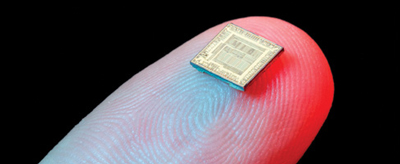 Rather than producing disposable probes or one-off ultra-sharp tips, Mesoscope engineers probes as durable measurement instruments. The goal is not maximum sharpness at any cost, but controlled, repeatable contact behavior that holds up across long analysis sessions, multiple operators, and different SEM platforms.
This philosophy directly addresses one of the most persistent problems in advanced-node failure analysis: data inconsistency caused by probe-induced variability. By designing probes that behave predictably over time, Mesoscope enables engineers to compare results across tools, sites, and process stages without introducing probing artifacts into otherwise controlled workflows.
That discipline, rather than headline specifications alone, is what elevates Mesoscope from a capable supplier to a top-tier nano-scale probe manufacturer.
Failure Analysis Conditions, Not Lab Ideals
Advanced-node failure analysis increasingly involves probing partially developed structures, early silicon, or devices still undergoing process tuning. Contact windows are extremely limited, electron-beam voltages are kept low to avoid damage, and even minor mechanical disturbances can alter device behavior.
In these environments, probes optimized primarily for extreme sharpness often become liabilities. Apex degradation, contact resistance drift, and surface instability accumulate across sessions, making it difficult to distinguish true device behavior from probing effects.
For wafer fab failure analysis teams, analytical labs, and OEM partners, this variability is unacceptable. Yield learning, return material analysis, and root-cause investigations depend on data that remains comparable over time. Mesoscope’s probes are designed specifically to survive these real FA conditions, not idealized demonstrations.
Precision Defined by Correlation
How is precision measured in SEM-based nano-probing workflows for advanced-node semiconductor failure analysis?
Mesoscope defines precision through correlation between imaging and electrical measurements, particularly for techniques such as EBAC, EBIC, and EBIRCH. These methods require clean, stable electrical contact that does not disturb the device under test or introduce measurement artifacts.
Rather than optimizing probes for abstract sharpness metrics, Mesoscope designs for controlled contact forces, predictable compliance, and stable electrical behavior. This ensures that electrical signals can be reliably correlated with physical structure and material behavior.
Reliability is measured by whether results remain consistent across long analysis sessions and multiple operators. Usability is defined by how seamlessly probes integrate into existing SEM-based nano-probing workflows, allowing engineers to focus on analysis rather than tool management.
Making Sub-Five-Nanometer Probing Practical
“It is relatively easy to fabricate something extremely thin once,” Harrington explains. “The real challenge is producing probes that are thin, mechanically stable, electrically consistent, and reproducible across batches.”
Sub-five-nanometer apex geometry is often presented as a benchmark in nano-probing. For Mesoscope, it is a manufacturing baseline rather than a marketing claim. The company has established stable mass production of probes with curvature radii below five nanometers, while prioritizing reproducibility and durability.
-
Our probe designs are shaped by the same FA challenges our customers face. If a probe cannot survive real failure analysis, it does not belong in our product line.
“It is relatively easy to fabricate something extremely thin once,” Harrington explains. “The real challenge is producing probes that are thin, mechanically stable, electrically consistent, and reproducible across batches.”
Mesoscope designs exclusively for SEM-based nano-probing environments, where beam interaction, contact force, and compliance must be tightly controlled. Probes are manufactured from 99.9 percent pure tungsten, selected for its predictable elastic response, stiffness, and stable electrical behavior under electron-beam exposure.
Engineering tradeoffs between apex sharpness, shank geometry, and compliance are deliberately balanced to minimize device disturbance and slow apex degradation. By treating probes as part of a system-level workflow rather than standalone tips, Mesoscope keeps sub-five-nanometer precision consistently usable across operators and laboratories.
Manufacturing Discipline That Sustains Performance
At the core of Mesoscope’s differentiation is its proprietary MSCT manufacturing process, which tightly controls electrochemical etching, apex formation, surface morphology, and shank geometry at the nanometer scale. The process eliminates common sources of variability found in conventional nano-tool manufacturing, including coatings, grain boundaries, and residual contamination.
A defining characteristic of the process is that probes are never exposed to electron beams during fabrication. This avoids beam-induced surface modification or latent damage that can compromise mechanical strength or electrical behavior before the probe ever enters a lab.
Strict regulation of etch parameters, current stability, and post-etch conditioning enables exceptional lot-to-lot consistency. Mesoscope maintains full traceability for every probe batch, is ISO 9001 certified, and treats quality control as an extension of engineering discipline rather than a compliance exercise.
Before shipment, customers receive SEM inspection images for every individual probe, along with detailed specification sheets and inspection reports. This transparency allows engineers to validate probe characteristics upfront, reducing uncertainty during critical failure analysis work.
Expanding Failure Analysis Beyond Probes
Why has Mesoscope expanded into comprehensive failure analysis services for semiconductor customers?
Mesoscope’s commitment extends beyond being the world’s premier nano probe manufacturer. The company is actively building a comprehensive, end-to-end Failure Analysis service capability grounded in decades of experience in electrical failure analysis and nano-scale measurement.
Customers engage Mesoscope as an outsourced partner when internal resources are constrained or workloads spike, relying on the team to manage overflow investigations and provide specialized nano-probing expertise without expanding in-house infrastructure. In practice, Mesoscope functions as additional bench capacity rather than simply a tool supplier.
Its FA portfolio spans optical microscopy, laser decapsulation, 3D X-ray inspection, PFIB, FIB, TEM, and SEM-based nano-probing. What makes this expansion meaningful is not simply the breadth of tools, but the depth of understanding behind them. Mesoscope connects physical, structural, and electrical data into coherent, actionable insight that accelerates root-cause identification.
This represents a long-term commitment to the semiconductor community to provide customers not only with best-in-class probing solutions, but also with integrated failure analysis services capable of supporting the most advanced technology nodes.
Why FA Capability Strengthens Probe Design
Mesoscope’s expansion into broader failure analysis services is not adjacent to its probe business. It is foundational to it and functions primarily as an internal engineering feedback loop rather than a shift in commercial focus.
Because the company performs failure analysis itself, its probe designs are exposed to real FA constraints, long sessions, marginal devices, and imperfect samples. This direct exposure feeds back into probe engineering, ensuring that designs survive actual analysis conditions rather than theoretical use cases.
“Our probe designs are shaped by the same FA challenges our customers face,” Harrington notes. “If a probe cannot survive real failure analysis, it does not belong in our product line.”
By connecting physical, structural, and electrical data across SEM, FIB, TEM, and related workflows, Mesoscope designs probes that reflect how failure analysis is actually performed, not how it is assumed to be done.
From Customer Feedback to Production Standard
The third pillar of Mesoscope’s R.P.I. philosophy, Improve, is driven by structured feedback from active labs. Input from scientists, engineers, and operators is evaluated systematically and correlated across multiple environments before being incorporated into production.
In one recent engagement, customers reported instability during low electron-beam voltage probing. Image adjustment became difficult, reducing operator confidence and compromising repeatability.
Rather than delivering a one-off fix, Mesoscope launched a structured investigation. Multiple probe variants were developed with controlled specification differences and evaluated under low keV conditions with partner labs. Performance was correlated across tools and operators to identify a stable configuration window. A second validation cycle confirmed consistent results, after which the optimized design was approved for large-scale procurement.
“Before, engineers struggled with unstable imaging and inconsistent contact at low keV,” Harrington says. “After deployment, performance stabilized across operators and tools, which restored confidence in the data.”
A Leadership View on What Comes Next
As device scaling continues, Harrington sees many nano-probing approaches failing not because they lack sharpness, but because they lack discipline.
“The industry is moving toward smaller contact windows and more sensitive measurements,” Harrington says. “Probes that are optimized for demonstrations rather than durability will struggle. The winners will be those who can deliver consistent data across time, tools, and people.”
 TrInity is Mesoscope Technology’s integrated solution for advanced semiconductor failure analysis, combining cutting-edge nano-probing, precision microscopy, and data-driven diagnostics. Designed to address increasingly complex device architectures, TrInity enables faster root-cause identification and higherresolution electrical characterization. It empowers customers with a comprehensive, scalable platform to accelerate innovation, improve yield, and support next-generation semiconductor development.
Mesoscope Technology has established itself as a long-term partner for advanced-node failure analysis by grounding nano-scale capability in repeatability, transparency, and manufacturing rigor. The R.P.I. spirit ensures that reliability, precision, and improvement remain operational priorities, not slogans.
For semiconductor leaders operating at the limits of device scaling, that consistency is not optional. It is the foundation of credible analysis and sustained trust.
| Share this Article:Tweet
|
Company
Mesoscope Technology
Management
Vincent Huang,Chairman
Description
Mesoscope Technology is a Taiwan-based manufacturer of nano scale probe tips, delivering precision solutions for advanced semiconductor analysis. Serving leading fabs and research labs, it specializes in ultra-fine probing technologies down to 5nm, enabling reliable measurement, failure analysis, and next generation device development.
This content is copyright protected
However, if you would like to share the information in this article, you may use the link below: