
Thank you for Subscribing to Semiconductor Review Weekly Brief
× 
Semi Conductor Review Weekly Brief
Be first to read the latest tech news, Industry Leader's Insights, and CIO interviews of medium and large enterprises exclusively from Semi Conductor Review
LongServing Technology has been recognized by Semiconductor Review Magazine as “Top 10 Photonic Quantum Computing Companies In Apac -2024” based on our proprietary methodology, reflecting its position in the industry. This profile has been developed by the Semiconductor Review research and editorial team based on insights from an interview with Dr. Ko-Cheng Fang, Inventor, Founder & Chairman.



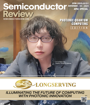
LongServing Technology
Illuminating The Future Of Computing With Photonic Innovation

 Dr. Ko-Cheng Fang, Inventor, Founder & Chairman
Leading this revolutionary shift is Dr. Ko-Cheng Fang, the visionary inventor, founder and chairman of LongServing Technology. Fang is redefining the limitations of traditional computing. His invention of the world's first multi-bit photonic chip—now patented in 20 countries—marks a monumental leap forward. This chip significantly enhances computing power and speed by harnessing photons instead of electrons, unlocking possibilities that were once out of reach.
Beyond groundbreaking hardware, he addressed the bottlenecks in conventional chip manufacturing by pioneering a picoscopic and nanoscopic-scale circuit design process. This novel approach eliminates the need for traditional lithography, dramatically improving the efficiency and scalability of integrated circuit (IC) chip production.
“Existing electronic chips using binary algorithms are insufficient to meet the computational demands of today’s AI era. Our multi-bit photonic computing chips enable high-speed processing, opening the door to the development of photonic CPUs and AI robots with high commercial value,” explains Fang.
So, how does this photonic chip revolutionize computing?
It replaces traditional electronic circuit boards with optical pathways, generating multi-frequency optical signals transmitted through optical modules. These signals are stored as a plurality of optical information. Upon receiving external commands, the stored data is retrieved, processed and outputted. This optical computing cycle is far more power- and energy-efficient than binary-based computing as it allows for multi-bit processing and eliminates the need for complex copper wiring and expensive extreme ultraviolet (EUV) lithography.
Fang's other groundbreaking invention is hailed as the “savior of Moore's Law.” His method reduces the line spacing in circuit patterns of IC chips to 0.1 nanometers—the diameter of an atom. This level of miniaturization allows the production of circuits on an atomic scale. 
The inventions have profound implications. As global tech companies grapple with the limitations of traditional computing and chip design, Fang's innovations signal the dawn of a new era.
Overcoming the Limits of Traditional Computing
As the demand for faster, more powerful computing intensifies, the constant pursuit of miniaturizing transistors has hit a critical impasse. For decades, semiconductor foundries have been shrinking transistor sizes to pack billions onto silicon chips, but now, the physical limitations of this miniaturization threaten to stall technological progress.
At the nanometer scale, traditional electronic chips grapple with quantum tunneling effects that lead to leakage currents. Astonishingly, at just a 1nm scale, nearly half of the electronic signals stray outside their intended circuits, resulting in signal ambiguity between binary values of ‘0’ and ‘1’ and impeding performance advancements.
The use of III-V semiconductor materials for logic gates exacerbates issues of overheating and high power consumption, especially during high-voltage applications. These challenges hinder the performance levels required for next-generation computing systems.
LongServing Technology’s photonic chip emerges as a more viable option for nanometer-scale architectures. Unlike their electronic counterparts, photonic chips use optical paths or photonic gates that are immune to the effects of interference, eliminating leakage currents and maintaining clarity and reliability in signal processing.
The magic behind LongServing Technology’s photonic chip lies in the manipulation of silicon's distinct properties to create optical pathways. The chip uses monocrystalline silicon as a photoresist material, restricting photon movement in a specific path. Simultaneously, polycrystalline silicon serves as the photosensitive material that amplifies the optical signals. This combination of silicon properties creates a highly efficient pathway for photons, eliminating the need for complex copper wiring or additional electronic components.
Breaking free from binary constraints, photonic chips transmit data using optical signals of varying wavelengths, enabling decimal (0-9) calculations.
This multi-bit capability accelerates data processing and enhances efficiency without the complexities associated with quantum superposition, refraction or diffraction. Varying the width of optical paths generates different signals, forming the basis for multi-bit calculations.
The innovative method employs pressurized electron beams and X-rays to create circuit patterns as small as 0.1 nanometers. Departing from conventional lithography that depends on large hydrocarbon molecular structures as photoresists, his approach eliminates the need for photoresists altogether.
“Our chip uses quantum dot materials with different wavelengths, which interact with the nanometer-width optical paths. This functions similarly to quantum computers, making our chip the ultimate solution for quantum and supercomputers,” says Fang.
To appreciate the leap forward, consider how traditional electronic chips operate. Transistors act like bridge piers, with electrons shuttling back and forth—each pass serving as a switch. This process inherently slows computation and increases power consumption. Materials like gallium nitride (GaN) and silicon carbide (SiC) are employed as photosensitive and photoresist materials, respectively, to create these switches when voltage is applied.
Take the number 81, which in binary is represented as 1010001. An electronic chip must toggle its transistors 'on' and 'off' multiple times to process this number, consuming significant energy. In stark contrast, a 10-bit photonic chip can represent '8' and '1' with just two flashes of light, dramatically boosting speed and energy efficiency.
Fang's original patent outlines that the ultimate goal is to replace existing chips with photonic CPUs and GPUs. This breakthrough heralds a new era where multi-bit photonic chips could become the cornerstone of a faster, more efficient foundation of future computing.
Breaking the Technology Barrier with a Revolutionary Approach to Chip Manufacturing
Creating nanoscopic or picoscopic scale circuit patterns in electronic chips is a complex and resource-intensive process, primarily driven by EUV lithography machines.
EUV machines cost millions of dollars each, consume vast amounts of electricity and suffer from low energy conversion efficiency. They generate a wavelength of 13.5 nanometers, which is sizable when the industry is aiming for circuit sizes of 5 nm, 3 nm, or even smaller. Reducing the wavelength to smaller scales involves complex, multi-step processes that grapple with diffraction limits and light overlap and demand extreme precision. Even the slightest misalignment can render a chip defective, making high yield rates a constant challenge.
But what if there were a way to bypass these obstacles entirely?
Fang’s groundbreaking patent, “Method of Making a Picoscopic Scale/Nanoscopic Scale Circuit Pattern,” promises to revolutionize chip manufacturing as we know it.
-
Our multi-bit photonic computing chips enable high-speed processing, opening the door to the development of photonic CPUs and AI robots with high commercial value
The innovative method employs pressurized electron beams and X-rays to create circuit patterns as small as 0.1 nanometers. Departing from conventional lithography that depends on large hydrocarbon molecular structures as photoresists, his approach eliminates the need for photoresists altogether.
“We use chemical reduction reactions to reduce photosensitive particles in the photosensitive layer,” explains Fang. “This allows for the easy formation of picoscopic-scale electronic circuit patterns or optical paths, eliminating the need for copper wire embedding, evaporation and etching.”
Since Fang’s patent uses X-ray technology, it can be likened to a photocopier and utilized to rapidly irradiate X-rays to mass-produce chips. By utilizing X-ray technology in this novel way, Fang's technique enables rapid mass production of chips without the exorbitant costs and energy consumption of traditional methods. This process also does away with the stringent operating conditions—like vibration-free, vacuum-clean rooms—that EUV lithography demands. X-rays penetrate soft materials while leaving denser substances intact, ensuring line precision even in less controlled environments and simplifying the production process.
As the semiconductor market teeters on the edge of explosive growth, Fang's innovation couldn't be timelier. The World Semiconductor Trade Statistics predicts an annual increase of $68 billion in 2024, pushing the total market value to $588.4 billion. In this booming landscape, Fang’s patent stands out as a potential game-changer, especially with authorized cooperative development on the horizon. It could unlock the ability to produce computing chips on a scale and at a cost previously deemed unimaginable.
Pioneering the Future of AI
As the age of AI continues to evolve, the demand for smaller, more powerful chips becomes increasingly urgent. LongServing Technology’s multi-bit photonic chip is a significant advancement that addresses this need.
Photonic bits can replace electronic bits, drastically reducing the number of required transistors and making chips of the same size thousands of times more efficient. Light-speed computing far exceeds electronic transmission, which greatly enhances the prospects of AI.
These high-speed calculations enable engineers to design machines that mimic the way the human brain processes information. For instance, machines can be programmed to perceive depth and spatial orientation and interpret the world from multiple directions—up, down, left, right and beyond.
“With our technology, computation mirrors human visual perception,” says Fang. “With the power of our photonic chips, creating realistic AI robots becomes feasible. Robots with these chips can operate like supercomputers, delivering the speed and processing power needed for life-like AI simulations.”
In the domain of autonomous driving, existing systems rely heavily on radar, LiDAR and vast satellite-driven calculations. However, by integrating photonic chips, the autonomous driving system can process information in 3D, make split-second decisions, and easily handle complex driving tasks.
In the surgical field, robots can perform delicate procedures with unparalleled accuracy. These robots are immune to fatigue, addressing shortages in medical personnel and alleviating the strain on healthcare systems. By assisting doctors, these robots can enhance surgical precision and improve patient outcomes.
Multi-bit photonic chips offer a compelling alternative to traditional quantum computers, particularly in capturing quantum signals. While quantum computers require superconductors operating at absolute zero or -273.15°C to avoid interference, photonic chips do not face these challenges. They provide a more stable, efficient environment without the complications of electronic interference or leakage currents.
The AI revolution is reshaping industries and economies on an unprecedented scale. According to the Optoelectronics Association, AI's influence will reach new heights by 2030. Precedence Research forecasts that global AI output will skyrocket from $100 billion to $1591 trillion, nearly 20 times its current value. Similarly, McKinsey Global Institute predicts AI’s economic impact will generate between $13 trillion and $15 trillion in output by 2030.
With LongServing Technology’s photonic chips, these ambitious figures are well within reach. The transition from electronic chips to photonic chips is an irreversible trend, and one could truly say that the era of photonics has finally arrived.
Shaping the Future of Computing with a Photonic Leap
With patents approved in key semiconductor regions such as Taiwan, China, the European Union, the United States, Hong Kong (SAR of China) and Japan, LongServing Technology’s chip has demonstrated its potential to replace traditional electronic components.
Following the public announcement of the chip, Fang noticed a surge in interest, with companies racing to develop their versions of photonic CPUs. Industry leaders and academic researchers have acknowledged that photonic CPUs and GPUs represent a pivotal advancement. Numerous countries are investing in research and development of photonic chips to remain competitive.
As Fang says, “Computing power is national power.”
His picoscale-chip manufacturing process has also caught the attention of major industry players like Intel and TSMC. Intel's CEO has recognized that future chip development will rely more on materials science advancements than machinery. TSMC shifted its focus from purchasing costly lithography machines to pursuing its “Angstrom chip” plan, inspired by Fang’s patent. LongServing Technology advocates for fair competition and patent licensing, as these principles are crucial for the evolution of human civilization.
Taiwan has made significant strides by transitioning from nuclear energy to greener alternatives in an attempt to curb carbon emissions. While this shift promotes long-term environmental sustainability and public health, it poses challenges for the technology industry as the demand for electricity rises alongside the growing need for more wafer fabrication labs. Adopting LongServing Technology’s photonic chip technology presents an opportunity to address these concerns.
By reducing the electricity consumption associated with chip production, photonic chips can enable tech companies to develop AI modules with greater computing power and energy efficiency while governments execute their green energy policies. With the world of computing brimming with technological advancement, Fang’s pioneering inventions align with global sustainability efforts and are a win-win for the tech industries and society.
Watch our video here: www.youtube.com/watch

| Share this Article:Tweet
|
Company
LongServing Technology
Management
Dr. Ko-Cheng Fang, Inventor, Founder & Chairman
Description
LongServing Technology, led by Dr. Ko-Cheng Fang, is revolutionizing computing with its patented multi-bit photonic chip technology and pioneering picoscopic-scale circuit design process. Its innovative photonic chip offers faster, more energy-efficient alternatives to electronic chips, addressing the limits of traditional computing. By enhancing AI development and promoting sustainability, LongServing Technology is at the forefront of next-generation semiconductor and photonic advancements.
This content is copyright protected
However, if you would like to share the information in this article, you may use the link below: