
Thank you for Subscribing to Semiconductor Review Weekly Brief
× 
Semi Conductor Review Weekly Brief
Be first to read the latest tech news, Industry Leader's Insights, and CIO interviews of medium and large enterprises exclusively from Semi Conductor Review
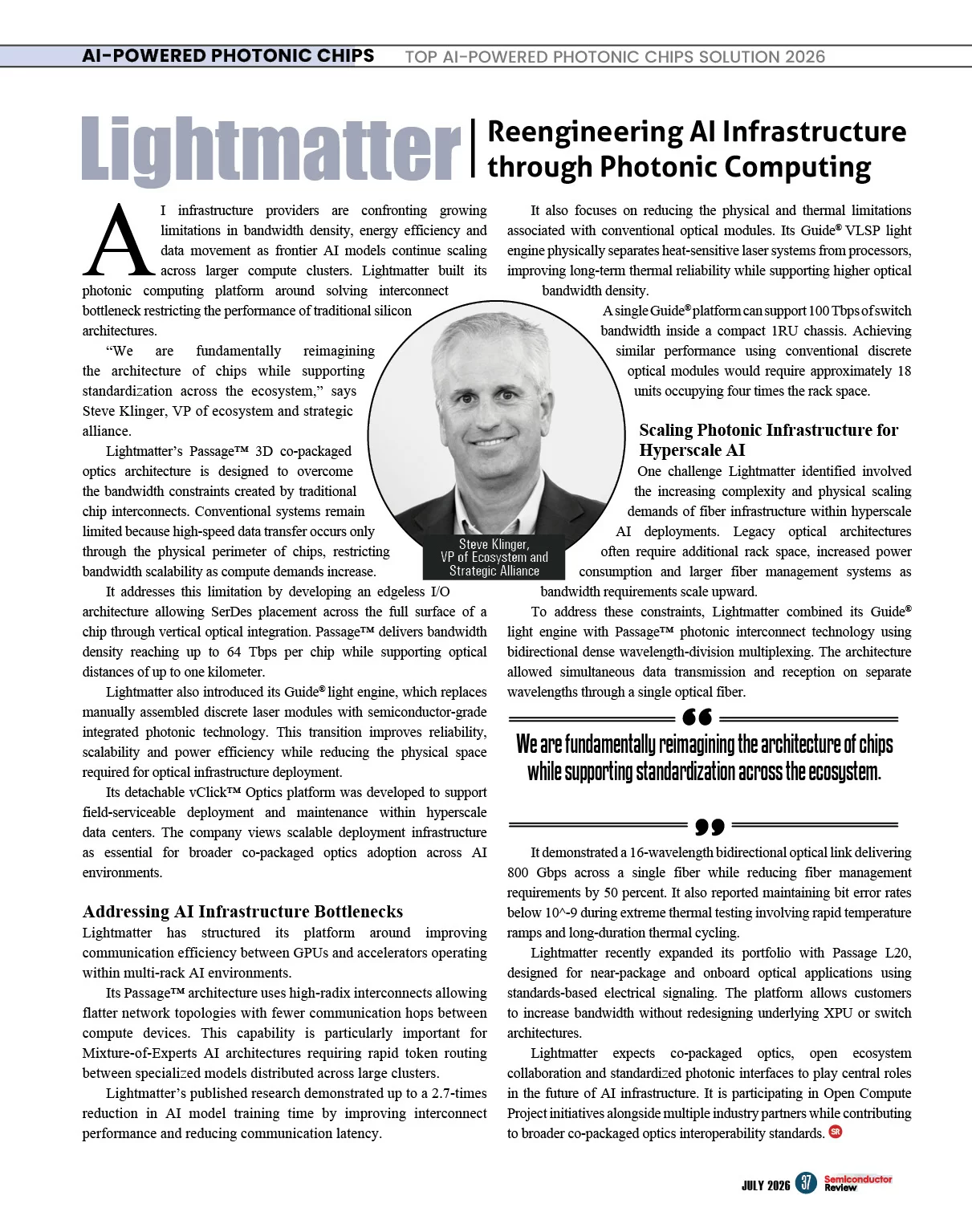
Lightmatter has been recognized by Semiconductor Review Magazine as the exclusive recipient of “Top AI Powered Photonic Chips Solution 2026,” based on our proprietary methodology, reflecting its position in the industry, and is also named among “Top Semiconductor AI Companies,” reflecting its broader leadership. This profile has been developed by the Semiconductor Review research and editorial team based on insights from an interview with Steve Klinger, VP of Ecosystem and Strategic Alliance.



Lightmatter
Reengineering AI Infrastructure through Photonic Computing

Lightmatter has structured its platform around improving communication efficiency between GPUs and accelerators operating within multi-rack AI environments.
Its Passage™ architecture uses high-radix interconnects allowing flatter network topologies with fewer communication hops between compute devices. This capability is particularly important for Mixture-of-Experts AI architectures requiring rapid token routing between specialized models distributed across large clusters.
Lightmatter’s published research demonstrated up to a 2.7-times reduction in AI model training time by improving interconnect performance and reducing communication latency.
 It also focuses on reducing the physical and thermal limitations associated with conventional optical modules. Its Guide® VLSP light engine physically separates heat-sensitive laser systems from processors, improving long-term thermal reliability while supporting higher optical bandwidth density.
A single Guide® platform can support 100 Tbps of switch bandwidth inside a compact 1RU chassis. Achieving similar performance using conventional discrete optical modules would require approximately 18 units occupying four times the rack space.
Scaling Photonic Infrastructure for Hyperscale AI
One challenge Lightmatter identified involved the increasing complexity and physical scaling demands of fiber infrastructure within hyperscale AI deployments. Legacy optical architectures often require additional rack space, increased power consumption and larger fiber management systems as bandwidth requirements scale upward.
To address these constraints, Lightmatter combined its Guide® light engine with Passage™ photonic interconnect technology using bidirectional dense wavelength-division multiplexing. The architecture allowed simultaneous data transmission and reception on separate wavelengths through a single optical fiber.
It demonstrated a 16-wavelength bidirectional optical link delivering 800 Gbps across a single fiber while reducing fiber management requirements by 50 percent. It also reported maintaining bit error rates below 10^-9 during extreme thermal testing involving rapid temperature ramps and long-duration thermal cycling.
Lightmatter recently expanded its portfolio with Passage L20, designed for near-package and onboard optical applications using standards-based electrical signaling. The platform allows customers to increase bandwidth without redesigning underlying XPU or switch architectures.
Lightmatter expects co-packaged optics, open ecosystem collaboration and standardized photonic interfaces to play central roles in the future of AI infrastructure. It is participating in Open Compute Project initiatives alongside multiple industry partners while contributing to broader co-packaged optics interoperability standards.
Selecting Photonic Chip Architecture for AI Scale
AI infrastructure buyers have learned that accelerator roadmaps do not solve the whole scaling problem. Larger clusters can expose a narrower, less forgiving constraint between processors, where bandwidth, reach, heat and service access begin to shape training economics as much as raw compute. Electrical links still matter, but their limits become more visible when model growth pushes traffic across racks rather than inside a single chassis. The buying question is no longer whether photonics can help. It is whether a photonic architecture can survive the production and maintenance pressures of hyperscale deployment.
Rack planning is now tied to interconnect design. More optical modules can add bandwidth, yet that approach can also add faceplate congestion, cable burden, power draw and thermal exposure. Dense AI fabrics need fewer avoidable hops between processors, especially when workloads route tokens across specialized compute pools. Latency penalties that look small at the component level can become expensive at cluster scale. A credible photonic chip approach must increase bandwidth density while reducing the packaging compromises that make deployment difficult after procurement approval.
Manufacturability deserves the same scrutiny as speed. Advanced packaging, wafer-level testing, supplier coordination and field replacement mechanics decide whether a design can move from technical promise to repeatable production. Permanent fiber attachments can create yield and service risk once expensive processors and switch chips enter final assembly. External light sources also carry tradeoffs. Keeping lasers away from hot processors can improve reliability, but only if the light engine is compact enough for real chassis layouts and controlled enough to handle wavelength management without delicate manual intervention.
Interoperability is another buying pressure, not a secondary feature. Hyperscale infrastructure is assembled across foundries, OSAT partners, interface IP providers and system vendors. A photonic chip design that forces wholesale package redesign creates adoption friction even when its physics are attractive. Buyers should favor architectures that support standard electrical signaling and accepted die-to-die interfaces while fitting into XPU or switch roadmaps. The strongest options will narrow the gap between lab performance and deployment discipline.
Serviceability may become the quiet test. AI clusters cannot treat optics as fragile custom assemblies hidden inside packages that are difficult to verify or repair. Detachable fiber interfaces, field access, known-good optical engines and earlier test points reduce the risk of discovering optical faults late in a costly build. Energy use still sits at the center of the decision, but power must be assessed alongside fiber count, chassis density, thermal separation and replacement workflow. A cheaper component can become expensive if it multiplies rack space or slows cluster bring-up.
Lightmatter stands out as a premier choice for buyers evaluating AI-powered photonic chips because its approach connects bandwidth with the practical mechanics of packaging and deployment. Its Passage platform addresses the shoreline bottleneck through 3D co-packaged optics and edgeless I/O, with versions reaching 32 to 64 Tbps of optical I/O per chip. Guide adds a semiconductor-grade VLSP light engine that reduces dependence on bulky discrete laser modules, while vClick Optics makes the fiber attach interface detachable for advanced packaging and field service. For buyers scaling AI clusters without forcing wholesale chip redesigns, Passage L20’s standards-based electrical signaling and BiDi multiplexing make Lightmatter a restrained, technically grounded recommendation.
...Read more
| Share this Article:Tweet
|
Company
Lightmatter
Management
Steve Klinger, VP of Ecosystem and Strategic Alliance
Description
Lightmatter develops photonic computing and co-packaged optics technologies for AI infrastructure environments. The company combines photonic interconnects, integrated optical engines and scalable semiconductor architectures to help hyperscale data centers improve bandwidth density, energy efficiency and AI model training performance.
This content is copyright protected
However, if you would like to share the information in this article, you may use the link below: