



Nokibul Islam
STATSChipPAC's XDFOI® Package: STATSChipPAC's RDL-based interposer package is named "XDFOI®" (X Dimension Fan Out Integration). This package family is designed for fan-out packages with heterogeneous integration. XDFOI® offers flexibility to package single or multi-functional chips, including logic, memory, power management, RF, and passive components, making it suitable for a wide range of applications. A simplified process flow for RDL-based XDFOI® technology is illustrated in Figure 1.
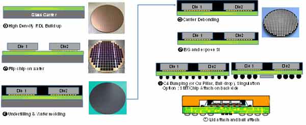
Figure 1: XDFOI® process flow for high pin count RDL-based package
XDFOI® technology was initially developed with RDL sizes up to 44x44mm and featured 4μm line and 4μm space dimensions. This served as an evaluation phase, likely involving test vehicles (TVs) to collect process data and assess long-term reliability.
Over time, the RDL reticle size extended to 55x55mm, providing a larger area for packaging solutions. Currently, XDFOI® technology offers more than a single reticle size, allowing for greater flexibility in packaging designs. Multiple reticle sizes, possibly with stitching techniques, are available. The newer iterations of XDFOI® technology feature finer line and space dimensions, with measurements as small as 2/2μm. This finer feature size enables more compact and densely packed designs, which can be advantageous for high-density and high-performance applications. The technology incorporates multi-stack vias, which allow for vertical connections between different RDL layers. This feature enhances the interconnectivity and routing capabilities of XDFOI® packages. Typical cross-section picture of a fine line and space XDFOI® with multi stack vias shown in Figure 2. In summary, XDFOI® technology has seen significant advancements since its initial development, with expanded reticle sizes, finer line-space dimensions, and the incorporation of multi-stack vias. These developments enhance its suitability for a wide range of packaging requirements; particularly those demanding high-density interconnects and intricate designs.
Figure 2: Typical cross-section picture of XDFOI® for 4LRDL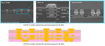
Embedded silicon bridge dies play a crucial role in improving the routing between different dies and between the die and memory in semiconductor packages. They enable localized fine interconnections without the need for increasing reticle size, which can be cost-effective and efficient. The use of embedded bridge dies can potentially reduce costs in the packaging process. This is significant, especially in high-volume manufacturing scenarios. Scalability is an important consideration in semiconductor packaging, particularly as the demand for higher performance and memory capacity increases. Embedded bridge dies offer a solution to scalability limitations in both silicon and RDL interposers. Embedded bridge dies are specifically designed to achieve finer routing density, which is essential for complex chip-to-chip and chip-to-HBM (High Bandwidth Memory) integration. This level of routing density is particularly beneficial for high-performance applications in fields like HPC, AI, and high-performance automotive electronics. Figure 3 provides a visual representation of a typical bridge die in an RDL interposer package, along with cross-sections showing how the bridge die is integrated using flip chip and micro bump joints.
Figure 3: Embedded bridge die and an RDL interposer package

Standard Multi-Chip Module (MCM) packages with build-up or laminate substrates are widely used in applications like high-performance computing (HPC), artificial intelligence (AI), and automotive electronics. These packages are suitable when ultra-fine pitch routing is not a strict requirement. While standard MCM packages have their advantages, they also come with limitations in terms of routing capability and certain electrical, thermal, and other properties compared to fine-pitch RDL-based substrates. High pin-count flip chip packages often face thermal challenges. To meet thermal requirements, a thermal lid along with a high thermal Bill of Materials (BOM) is sometimes necessary for flip-chip packages. In the case of a module where the die power is not high, there may be no need for an expensive thermal lid and thermal BOM. Some module packages for low-power applications are non-lidded.
RDL fan-out packages are typically more expensive than laminate substrate packages. The cost can further increase when embedded bridge dies are added to the RDL package. Embedded die is only necessary when the RDL substrate alone cannot complete the required routing between die-to-die and die-to-memory. RDL packages, with or without embedded dies, are generally less expensive than silicon interposer-based packages. This makes them a cost-effective option for many high pin-count applications. Figure 4 shows various Chiplet packaging options along with relative cost data. Such data are helpful for understanding the cost implications of different packaging choices.
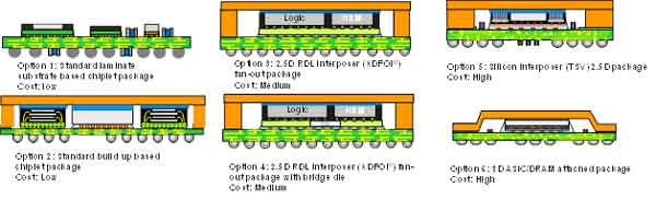
Figure 4: Various options of Chiplet package and relative cost data
