


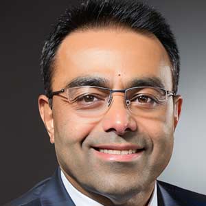
Osman Sorkhabi
Currently serving as a Director of Engineering at Lam Research, Osman Sorkhabi has devoted over two decades to the semiconductor industry. After earning a PhD in Physical Chemistry from the University of California, Davis, Dr. Sorkhabi entered the industry through a role at Therma-Wave, which marked the beginning of an extensive career in semiconductors.
Subsequent positions at Tokyo Electron, Spansion, and Western Digital provided Dr. Sorkhabi with a rich breadth of experience across the industry. As part of the teams at these organizations, Dr. Sorkhabi contributed to significant projects and initiatives that drove both innovation and efficiency in semiconductor manufacturing and R&D.
Another significant aspect of Dr. Sorkhabi 's career has been her/his contribution to scientific research. With over 42 peer-reviewed publications to his name, Dr. Sorkhabi 's work has deepened the understanding of the field and provided new paths for exploration. He also holds four patents, underlining his inventive thinking and commitment to pushing the boundaries of tech innovation.
Could you provide an overview of your role and responsibilities within the company?
I am currently Director of Engineering at Lam Research in the Corporate Metrology group. In this capacity, I spearhead projects across multiple organizations and geographies, delivering innovative technology solutions while meeting aggressive timelines. Some key aspects of the job are to establish strategic relations, influence key decisions, and lead talent development initiatives to achieve organizational goals.
What are some of the key challenges you face?
As the semiconductor industry adopts more complex memory and logic architectures, we’re seeing challenges emerge not only on the process side for making the devices, but also in metrology to measuring them. Since my focus is on metrology, we need to stay ahead of the curve and anticipate challenges. This means identifying technical gaps and developingtimely solutions.An example to consider arethe challenges for gate all around (GAA) architectures. The short-channel effect and its accompanying current leakage become problematic as 2D structures get smaller beyond the 3nm technology node. To overcome this, new architecturesare being introduced in logic applications to go from 2D to 3D by vertically stacking GAA transistors. From a metrology perspective, how do you measure such structures? What techniques do you use? Are there commercially available technologies that can do the job or do new one need to be created? That’s just one challenge in logic.We face similar challenges in memory – as the architecture gets more complex so does the metrology requirements.
“In technology, there will always be failures and setbacks. This is where persistence and perseverance come in. They help you to push through the hard times and to use them as learning experiences”
What would you say are some of the futuristic trends that will have an impact in the next 18-24 months?
Over the next 18-2 months, emerging trends in 3D DRAM and 3D NAND are the ones to follow. In July, Micron announced their 232-layer 3D NAND technology boasting twice the read/write speeds with 25% more efficiency. This came on the heels of SK hynix's announcement of their 238-layer 3D NAND product with 50% performance boost and 34% decrease in bit costs. These devices are designed with peripheral under cells (PUC) layout; similar to Micron's CMOS-under-array (CUA). The advantage of these layouts is that more memory can be squeezed into a tighter space while decreasing die size. These architectures pose significant challenges to established metrology techniques currently in use for measuring 3D NAND etch profiles such as CDSAXS and OCD. The presence of PUC/CUA affects the measurement signal and needs to be deconvoluted from the multilayered film stack above. Other challenges in are that tallerstacks in 3D NAND pose challenges to etching high aspect ratio holes. Cryogenic etch is being introduced to mitigate some of these challenges. Metrology will play a critical role in the development of these new architectures.
What advice would you give to young professionals who are interested in pursuing a similar career, and what qualities do you think are essential for success in this field?
A common advice is to ‘follow your passion’. But I think there’s more to it. It’s important to enjoy your work. I think it’s equally important to be persistent and to persevere. The ‘passion’ part will push and motivate you. But in technology, there will always be failures and setbacks. This is where persistence and perseverance come in. They help you to push through the hard times and to use them as learning experiences. The advice I’d give to young professionals is that if you’re passionate about technology and engineering, come work in the semiconductor industry. There are numerous grand challenges that remain to be solved. With persistence, creativity, and hard work we can solve them. For these reasons, it’s an exciting time to be part of this industry and the future technologies that it will enable.
