
Thank you for Subscribing to Semiconductor Review Weekly Brief
× 
Semi Conductor Review Weekly Brief
Be first to read the latest tech news, Industry Leader's Insights, and CIO interviews of medium and large enterprises exclusively from Semi Conductor Review
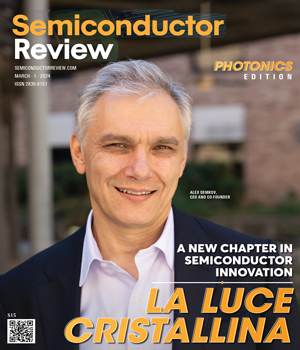
La Luce Cristallina has been recognized by Semiconductor Review Magazine as “Top 10 Photonics Solutions Companies - 2024” based on our proprietary methodology, reflecting its position in the industry. This profile has been developed by the Semiconductor Review research and editorial team based on insights from an interview with Alex Demkov, Ceo And Co-Founder.



La Luce Cristallina
A New Chapter in Semiconductor Innovation
 Alex Demkov, Ceo And Co-Founder
La Luce Cristallina (LLC) is at the forefront of this transformation, emphasizing the integration of crystalline functional oxides in semiconductor applications. LLC’s mission is summed up in its motto to drive innovation in semiconductor technology through the integration of crystalline oxides on silicon and other semiconductors. This approach leverages the diverse electronic, optical, and mechanical properties of thin film crystalline oxides, promising a revolution in the semiconductor industry. Their initial offering is the fabrication of specialty 8- and 12-inch wafers of strong electro-optic material that is fully compatible with CMOS foundries.
Unlocking Limitless Functionality through Novel Materials in Semiconductors
The challenge for the integration process is to introduce the rich attributes of complex oxides into the established silicon manufacturing framework. Achieving an atomically precise interface between the semiconductor and the oxide through some kind of template is important. This foundational layer paves the way for depositing additional suitable oxides, fostering a symbiosis of complex oxides with silicon’s robust platform.
 The interfacing between semiconductors and functional oxides is groundbreaking. It enables multifunctional, cooperative devices on the same die, heralding a new era of semiconductor device innovation via interface engineering with functional oxides. La Luce Cristallina’s pioneering work addresses current silicon limitations and paves the way for the next generation of semiconductor technology.
“The choice of material in photonic devices significantly impacts size and power requirements,” says Alex Demkov, CEO and co-founder of La Luce Cristallina.
The firm has made significant strides in the inorganic, electrooptical, active materials domain, where it integrates functional oxides with silicon and other semiconductors. Its main goal is to strike a balance between improved electro-optic performance and cost-effectiveness. Beyond photonics, they have also made strides in other fields, including power electronics via gallium oxide, and supplying wafer-scale substrates for Ambature, Inc., a company that makes high-temperature superconductor devices.
Flagship Innovation
One of La Luce Cristallina’s remarkable achievements is the development of optical grade epitaxial barium titanate (BaTiO3) on silicon wafers. This flagship product is affordable and delivers superior performance over purely silicon-based technology, as evidenced by lower power consumption, smaller footprint, and enhanced reliability. Barium titanate has a very high electro-optic coefficient, outperforming competitors (including lithium niobate and electro-optic polymers) and setting a new industry standard.
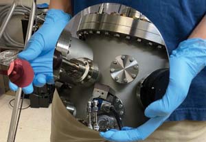 Traditionally, epitaxial barium titanate has been integrated into silicon by means of molecular beam epitaxy (MBE), a precise but time-consuming method for crystalline thin film growth. However, MBE has its limitations, especially when producing thicker films needed for optical applications, as these typically become highly oxygen-deficient and conductive, leading to potential device failure. La Luce Cristallina has addressed this issue by adopting off-axis RF sputtering, efficiently producing high-quality, optical grade, fully insulating crystalline films. This method ensures film quality and makes the next generation of SiPh more accessible and affordable.
 -
The choice of material in photonic devices significantly impacts size and power requirements
La Luce Cristallina differentiates itself in the market by focusing on barium titanate over other materials like indium phosphide and lithium niobate, which, while effective, are more expensive to produce and have size constraints for full wafers. The company’s decision to use barium titanate, a practical and safe material for mass production, reflects its commitment to providing high-performing and environmentally conscious solutions. Notably, barium titanate displays strong electro-optical properties, with a significantly higher (>20x) electro-optic coefficient than lithium niobate. Barium titanate eliminates the environmental and health hazards associated with other competing materials such as lead titanate and its solid solutions.
Advancing Crystal Growth Techniques
Incorporating barium titanate onto silicon wafers has been a viable practice for years, chiefly attributed to molecular beam epitaxy (MBE), a foundational technique in III-V semiconductor fabrication. Despite its established status, MBE’s ultra-high vacuum deposition process is known for its high cost of operation and slow deposition rate. In addition, MBE systems demand meticulous management in industrial settings due to their more frequent maintenance requirements.
We aim to leverage the unique and exciting functionalities inherent in complex oxides
In optics, the relatively large wavelength of light presents a unique challenge, necessitating thicker films for guiding and confinement with minimal loss. This requirement delineates two predominant alternatives—employing bulk crystals or investigating alternative film deposition methodologies. While bulk crystal modulators prove functional, their large size and high power consumption are notable drawbacks.
In response to this issue, La Luce Cristallina has developed a method to deposit optical grade barium titanate on strontium titanate-buffered silicon. This avant-garde technique ushers in a new era of effective light modulation using “thinner” films, presenting a more compact and energy-efficient alternative than conventional bulk crystal modulators.
The approach builds on researcher Rodney McKee’s innovation, which skillfully introduced a technique to safeguard silicon from oxidation during the epitaxial growth of an oxide crystal. Once this epitaxial oxide buffer layer is in place, subsequent crystalline oxide growth on silicon is less stringent. Instead of using ultrahigh vacuum methods, off-axis RF sputtering, well-known for its reliability, scalability and industrial applicability, is used by La Luce Cristallina for barium titanate. This technique efficiently addresses the film’s oxygen deficiency produced by ultra-high vacuum techniques such as MBE, ensuring insulating characteristics and mitigating parasitic currents during voltage modulation, curbing power losses. This approach retains the electro-optical efficacy of MBE films while also speeding up the growth by 10-20 times, resulting in high-performing electro-optical modulators without sacrificing manufacturability.
Although not as fast as conventional sputtering techniques, La Luce Cristallina’s method vastly outperforms MBE. This expedited process is critical, especially given the time required to cultivate optical-grade barium titanate films, which typically take several days to achieve thicknesses ranging from 0.2 to 0.5 microns needed for optical applications. Due to its considerably enhanced deposition rate, this innovative technique produces multiple wafers of such thickness in a single day.
Pioneering Advancements in Complex Oxides Integration
The team at La Luce Cristallina has been at the forefront of developing sophisticated deposition techniques for the past 15 years, as it revolutionizes the integration of functional oxides with silicon and other prevalent semiconductors. While initially focused on electro-optical modulators, the company’s aspirations extend beyond this sector.
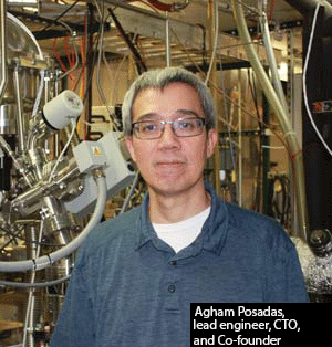
“We aim to harness the distinct and compelling features of complex oxides,” says Agham Posadas.
The adaptability of these oxides paves the way for myriad applications, far more than previous limitations of microscopic crystals or ultra-thin layers. La Luce Cristallina distinguishes itself by adeptly incorporating these materials into relatively thicker films that range from half a micron to two microns. This breakthrough enables the monolithic deposition of these robust films onto silicon substrates, combining the extraordinary attributes of oxides with semiconductor technology. The firm excels in producing largearea wafers, initially with its two-inch wafers, but utilizing its scalable deposition technique to accommodate a wide range of wafer sizes including 8- and 12-inch wafers, expanding the number of potential applications and market opportunities.
A Sustainable Approach: Prioritizing Performance and Environmental Consciousness
A significant clientele includes research and development divisions within some of the leading companies manufacturing optical transceivers for data centers. They procure the company’s product for material qualification and examine whether integrating the barium titanate on silicon aligns with their strategic directions. It not only collaborates with industry leaders in optical transceivers but also with many universities that do research on advanced technologies. La Luce Cristallina’s wafers are being evaluated by major manufacturers of electro-optical modulators, which are critical components of next generation data center transducers, which link optical fibers from transatlantic cables and servers. These wafers provide a significant advantage by enabling devices that consume far less power than conventional materials and that are compact enough to be suitable for use in co-packaged optics.
The demand for fast, high-frequency devices becomes paramount in response to the exponential growth in network capacity and data rates. The challenge lies in managing power consumption, especially when dealing with high-frequency charge modulation, which traditionally incur significant power costs. Barium titanate, known for its efficient modulation, enables short-distance light driving, creating ultracompact, low-power modulated regions. La Luce Cristallina’s initial focus is on the lucrative data transducer market for data centers, while at the same time, its research and development efforts are directed towards collaborating with those developing quantum and neuromorphic optical computing structures.
La Luce Cristallina aims to scale up production to 8-inch or 12-inch wafers in the next year. Once achieved, it predicts a shift in usage as customers leverage foundries to mass-produce their devices and chips. The goal is to build a strong presence in the barium titanate market, favorably positioning it for when the broader industry adopts this technology.
| Share this Article:Tweet
|
Company
La Luce Cristallina
Management
Alex Demkov, Ceo And Co-Founder and Agham Posadas, lead engineer, CTO, and Co-founder of La Luce Cristallina.
Description
La Luce Cristallina developed inorganic electro-optical active materials, specifically in the ferroelectric category, that can be seamlessly integrated into silicon at a reasonable cost.
This content is copyright protected
However, if you would like to share the information in this article, you may use the link below: