
SEMICONDUCTOR REVIEW THANK YOU FOR SUBSCRIBING
× 
Semi Conductor Review Weekly Brief
Be first to read the latest tech news, Industry Leader's Insights, and CIO interviews of medium and large enterprises exclusively from Semi Conductor Review
Semiconductor Review: Specials Magazine
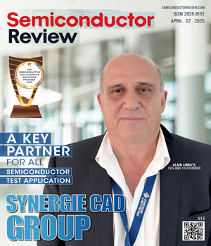
Synergie Cad Group
A Key Partner For All Semiconductor Test Application
Before a semiconductor can change the world, it must pass the ultimate test—an evaluation of its performance, reliability, and efficiency. Yet, in an industry where cutting-edge technology evolves at breakneck speed, true reliability and deep expertise are often in short supply. That’s where Synergie Cad Group comes in. As a leading designer and manufacturer of semiconductor test interface solutions, the company remains committed to its mission: to be a total solutions provider for semiconductor test development across all aspects of its business. Synergie Cad Group offers Test Interface Boards for automated test equipment (ATE), exploiting the full in-house capabilities for board design, printed circuit board (PCB) fabrication with leading edge technologies in its two sites in France and Vietnam, component assembly, and Wafer Probing Solutions in partnership with Nidec Advance Technology. The company also provides systems and applications for Reliability Test and Burn-In, covering the most challenging requirements in terms of device complexity and power consumption, in a wide spectrum from Automotive to HPC and AI applications. Additionally, Synergie Cad Group offers test development, industrialization and production services from its facility in Toulouse, which includes IC packaging design as part of its turnkey solutions. It specializes in complex and high-end designs, including RF, multiple-die configurations like SiP, and intricate substrates such as cavity designs. The Synergie Cad Group Advantage What makes Synergie Cad Group the preferred choice for those seeking reliability, efficiency, and cutting-edge innovation in semiconductor applications? Its deep expertise in semiconductor testing and reliability. But beyond technical excellence, its greatest asset is the strong relationships it has built with Tier 1 customers over the years. The company’s engineers work closely with customers, gaining firsthand insights into emerging technologies, testing requirements, and real-world challenges. This proximity enables it to anticipate market needs rather than merely react to them. The rapid evolution of semiconductor technology—where complex, integrated systems require balancing thermal, mechanical, and electrical considerations—demands a level of expertise beyond traditional PCB manufacturing. Unlike companies that simply supply PCBs or interface boards, Synergie Cad Group prioritizes application-driven solutions. By understanding how its products are used in the field, it delivers cost-effective, high-performance, and time-efficient solutions.
Photonics
Canyon Materials, Inc. (CMI), a leader in photonic innovation, has long been at the forefront of advancing grayscale lithography through its patented All-Glass Grayscale Photomask technology. Under the leadership of President Chuck Wu, the company has developed and supplied cutting-edge solutions that enable the creation of intricate 3D microstructures, revolutionizing industries ranging from optics to space exploration. “Founded on the principle of fostering technological advancement, we specialize in producing HEBS-glass (High-Energy Beam Sensitive glass) and LDW-glass< (Laser Direct Write glass) grayscale photomask blanks,” says Wu. These all-glass products are celebrated for their precision and versatility, offering unparalleled accuracy in both mass production and research applications. Among CMI’s many accolades is the prestigious Photonics Circle of Excellence Award< in 1997, underscoring the impact of its innovations. CMI’s HEBS-glass and LDW-glass grayscale photomasks have been utilized by prominent organizations, including NASA, Panasonic, Samsung, and the Smithsonian Observatory. The applications of these photomasks span a broad spectrum, from fabricating micro-optical elements like microlens arrays to crafting apodization filters. For instance, NASA’s Jet Propulsion Laboratory (JPL) used CMI’s HEBS-glass photomasks to develop an apodization filter that enabled the observation of Earth-like planets across vast cosmic distances.


Coherent Corp., a leading global provider of laser-based solutions and photonic technologies, has carved a niche for itself in a rapidly evolving technological landscape. The company specializes in delivering advanced lasers and optics for a broad range of industries, including industrial, communications, aerospace, defense, and life sciences. With a rich history of innovation, Coherent has continually evolved to meet the demands of the modern world, establishing itself as a critical player in the photonics sector. Founded in 1966, Coherent began as a research-focused company aimed at pioneering laser technology. Over the years, it expanded its offerings and expertise, transitioning from a research entity into a globally recognized provider of laser solutions. Coherent’s products include lasers, optics, and other photonic components that play an integral role in various applications, ranging from semiconductor manufacturing to medical diagnostics. In 2020, Coherent made a significant strategic move by acquiring II-VI Incorporated, a global leader in engineered materials and optoelectronic components. This merger expanded Coherent's portfolio and strengthened its position in the market, particularly in the semiconductor and communications industries. The combination of Coherent's cutting-edge laser technology and II-VI’s complementary materials science and expertise positioned the company to deliver more advanced, reliable, and efficient solutions for a broader customer base. This merger was a defining moment in Coherent’s growth trajectory, allowing it to tap into new growth markets while enhancing its R&D capabilities. Today, Coherent Corp. operates in a highly competitive global market, where it stands out for its continuous innovation and commitment to meeting the needs of its diverse clientele. Its product range is known for precision, reliability, and high performance. From its advanced lasers used in medical treatments and diagnostics to its cutting-edge technologies that enable high-speed data transmission and communication, Coherent remains a cornerstone of the photonics and laser industries. Under the leadership of CEO Jim Anderson, Coherent has embraced a forward-looking approach, investing in the future of photonics and laser technology. Anderson, who has been at the helm of the company since 2020, brings extensive experience in driving growth and operational excellence. His leadership has been instrumental in Coherent’s strategic expansion and its ability to navigate an increasingly dynamic and competitive market.
Intellectual Property

Harnessing the Power of Additive Manufacturing to Advance Semiconductor Capital Equipment Performance
Scott Green, Director Advanced Software R&D, 3D Systems Corporation
Electronic Contract Manufacturing

World Class Manufacturing Plant and Operational Excellence
Laurent Tarnaud, Director Operation Lithium & Director Advanced Manufacturing Engineering, Trojan Battery Company
Power Electronics

How to Make the Most of your Process Failure Mode and Effects Analysis
Monte Heisler, Director, Manufacturing Quality, North American Stamping Group
Semiconductor Testing and Quality Assurance

Advancements In Semiconductor Test Interfaces
Ben Buchanan, Director of Digital Design, Analog Devices (ADI (NASDAQ))
Photonics

An Operator Walks Up To A Machine Tool
Paul Guerrier, Manufacturing Engineering Manager, Moog Inc. (NYSE: MOG.A)

IN MY OPINION
Semiconductor Tech
Navigating Complexity: The Unsung Heroes Within
Rory Hepner, Directory Global Vehicle Logistics and Customs Operations, Mercedes-Benz (ETR: MBG)

LAST WORD
Electronic Contract Manufacturing
Smart Factory and Technical Skills Revolutionizing the Automotive Industry
Thales Souto, Manufacturing Engineering Manager, TE Connectivity
IN FOCUS
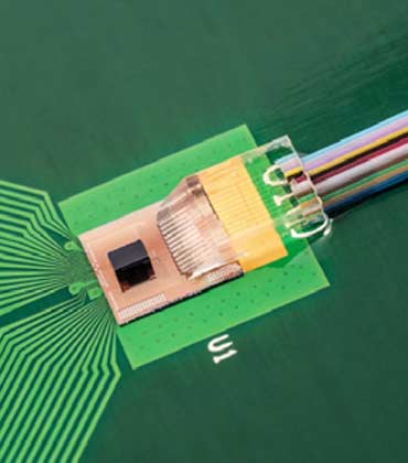
How Photonics is Revolutionizing Data Transfer
The increasing demand for accelerated data processing and transmission pushes conventional electronics to their limits.

EDITORIAL
Paving the Way for NextGeneration Technologies
In the world of modern electronics, semiconductors are the cornerstone of virtually every device that we rely on daily. From smartphones to advanced computing systems, these tiny components play an essential role in making electronic devices efficient, powerful, and increasingly smaller. As we continue to push the boundaries of technology, the integration of photonics with semiconductor testing interfaces has become a critical component in shaping the future of electronics.
At the heart of semiconductor testing lies the process of evaluating and validating the performance of individual semiconductor devices. This is a crucial step in ensuring that chips meet the desired specifications before they are incorporated into larger systems. Traditionally, semiconductor testing has relied on electronic-based test interfaces that use electrical signals to evaluate the behavior of the components. These interfaces are essential for diagnosing faults, ensuring reliability, and confirming that chips function properly under various operating conditions.
However, as semiconductor technology has advanced, the need for more sophisticated and faster testing techniques has arisen. The industry is continuously striving to meet the demands for chips that operate at higher speeds, handle more data, and consume less energy.
Photonics holds enormous promise for the semiconductor industry due to its inherent ability to handle large amounts of data at extremely high speeds with minimal energy consumption. By incorporating photonics into semiconductor test interfaces, manufacturers can achieve faster data transmission rates, which are especially important in testing chips used for applications like 5G, artificial intelligence (AI), and the Internet of Things (IoT).
The convergence of semiconductors, test interfaces, and photonics is opening new frontiers in electronics. The integration of photonics into semiconductor testing promises faster, more accurate, and more energy-efficient solutions, which are critical for meeting the growing demands of modern technology. As industries such as 5G, AI, and quantum computing continue to evolve, the importance of this fusion of technologies will only increase. Photonics, alongside semiconductor test interfaces, is poised to play a central role in shaping the next generation of electronic devices and systems that will define the future of technology.
This content is copyright protected
However, if you would like to share the information in this article, you may use the link below:
https://www.semiconductorreview.com/edition/april-2025-11.html