


Thank you for Subscribing to Semiconductor Review Weekly Brief
× 
Semi Conductor Review Weekly Brief
Be first to read the latest tech news, Industry Leader's Insights, and CIO interviews of medium and large enterprises exclusively from Semi Conductor Review
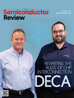
Deca Technologies has been recognized by Semiconductor Review Magazine as “Top 10 Semiconductor Tech Solution Companies - 2020” based on our proprietary methodology, reflecting its position in the industry. This profile has been developed by the Semiconductor Review research and editorial team based on insights from an interview with Tim Olson, CEO, Lori McDonald, Business Office Manager, Jan Kellar, Sr. Director Design Applications and Craig Bishop, CTO.


 Tim Olson, CEO, Lori McDonald, Business Office Manager, Jan Kellar, Sr. Director Design Applications and Craig Bishop, CTO
While it’s safe to assume that such possibilities will remain only in the realm of fiction for now, interestingly, a similar idea can already be observed in modern computing and the semiconductor industry. As the individual components of integrated circuits have been shrinking over the years, the maximum number of transistors that can be placed on a chip has been exponentially increasing. However, the extent to which these components of ICs can be miniaturized is about to hit a plateau.
So far, chip scaling has followed a simple linear curve that has stayed true to Moore’s prediction (the number of transistors per chip roughly doubles every two years) and scaled at 0.7x every two years. However, Moore’s law is finally on the verge of a technological singularity with component sizes reaching the atomic scale. It is thus imperative for the semiconductor industry to think beyond traditional monolithic ICs. Enter Deca Technologies, or more popularly, Deca, a company on a mission to re-architect the way the semiconductor industry creates advanced chips and electronic systems.
Think Different, Think Deca
“Our name ‘Deca’ stands for ten in Greek, signifying our passion to deliver order-of-magnitude breakthroughs in electronic systems through advanced chip interconnects,” says Tim Olson, founder, and CEO of Deca Technologies. We dug a little deeper to see what ‘Deca Difference’ the company has to offer.
Deca helps clients break free from the limitations and boundaries of monolithic ICs. For this, the company connects heterogeneous chiplets (smaller chips) and creates advanced non-monolithic systems on a chip (SoCs). If the idea sounds complicated, let us turn to Deca to break it down.
Olson elaborates that since the dawn of the integrated circuit, designers have successfully been pushing historic boundaries to create massive SoCs (systems on a chip) upon a single monolithic piece of silicon. While SoCs have incorporated an ever-growing number of processor cores, IO functionality and other functions, system dynamic memory has remained off-chip requiring high bandwidth signaling to occur through a PCB (printed circuit board).
Additionally, the growing size of SoCs and increasing cost in advanced technology nodes has placed increasing commercial pressure on IC designers to search for new ways to create highly integrated advanced electronic systems.
Since the creation of the company, Deca has thought differently with a focus on integrating disparate functional circuit blocks (heterogeneous functions or chiplets including memory) within an organic encapsulation material rather than depending only on monolithic silicon. Deca’s approach is called fan-out technology, specifically, FO-WLP (fan-out wafer level packaging) where electronic interconnect (or fan-out fabric) is laid upon the encapsulated chiplets to create ever higher performance systems in a cost-effective manner. As a result, IC manufacturers can continue scaling past the monolithic silicon plateau and enjoy multiple benefits of the chiplet approach including; higher levels of integration, shorter design cycles and faster time-to-market with chiplets optimized per technology node for yield and cost.
M-Series™ FX and Adaptive Patterning: The Future of Advanced Electronic Systems
Notably, the proof of Deca’s concept lies in its technology offerings—M-series and Adaptive Patterning® have been broadly adopted in the global Smartphone market. The company’s flagship M-Series is a patent-protected chips-first, chips-up, rugged, fully molded FOWLP technology that provides exceptional quality and reliability in a miniaturized format. With parallels, yet important distinctions vs. industry giant TSMC’s integrated fan-out (InFO) wafer-level packaging, M-Series provides exceptional electrical and thermal benefits in the smallest possible form factor. Through Adaptive Patterning and the associated production infrastructure, M-Series additionally provides a highly costeffective solution. To this extent, the awardwinning M-Series FX has already been designed into diverse high-volume mobile applications worldwide, delivering record-setting product performance. The recent introduction of Deca’s second generation 2μm technology node with the expansion to the new 600mm standard panel size greatly expands the market application space for M-Series to include high-performance computing (HPC), advanced networking, artificial intelligence (AI), and edge computing applications.
-
“Our name ‘Deca’ stands for ten in Greek, signifying our passion to deliver order-of-magnitude breakthroughs in electronic systems through advanced electronic interconnect,” says Tim Olson, founder and CEO of Deca Technologies

In providing more detail on Deca’s novel Adaptive Patterning, Olson noted “What makes it unique is the highly integrated nature of design rules and methods, design automation in both office and factory environments as well as amazing realtime systems which create optimized unitspecific patterns for every wire on every chip on every wafer or panel. We are the first company in the world to extend classic DFM (design for manufacturability) concepts into real-time DDM (designduring- manufacturing)!” Adaptive Patterning is a patented protected electronic design automation (EDA) system that provides unprecedented capability for manufacturers to accommodate natural variation in manufacturing vs.
 Liberty Perez, Director of Factory Automation and Cliff Sandstrom, VP of Technology Development
style=margin:right=5px;float:left;margin-right:10px;>Adaptive Patterning combines a high-speed, highly accurate optical position inspection with proprietary real-time design methods and a scalable computing cluster to generate a bespoke layout for each chiplet that compensates for measured positional error. In turn, these chiplets can operate with the best possible electrical performance while consistently achieving near 100 percent yield. Olson adds, “Our Adaptive Patterning system combines precise alignment functionality with real-time dynamic auto-routing and can operate in a system with even tens of thousands of high-frequency connections.”
When combined with Adaptive Pattering, M-Series’ design rules provide the largest ‘via’ contacts on the smallest chip interconnects. The planar M-Series surface is perfect for building highly integrated fan-out SoC structures. Scaling down to 2μm lines and scaling up with multiple redistribution layers (RDL) provides powerful new possibilities for IC designers partitioning silicon functional blocks into chiplets.
Creating More Opportunities through Collaboration
Deca’s innovations have been a runaway hit in the semiconductor industry. M-Series and Adaptive Patterning have established a new industry standard with multiple customers designing test vehicles across multiple future application spaces.
Through divestiture of its manufacturing operations in early 2020, Deca has transformed itself into a pureplay technology provider. Industry leading semiconductor producers and end product OEMs can now engage with Deca in an open innovation network from product design through manufacturing of chips at top-tier foundries. Equipment manufacturers can join the AP Live Network through technology supply and license agreements (TSLAs), providing certified AP Connect functionality across essential process steps to their end-users. Simultaneously, foundry service providers and manufacturers can access the Adaptive Patterning and M-Series technologies through technology transfer and license agreements (TTLAs).
It is also important to note that Deca has existing technology and license agreements with ASE Group (Advanced Semiconductor Engineering Inc.), the largest outsourced semiconductor assembly and test company (OSAT) in the world, and nepes Corporation, a leadingedge provider of wafer and panel-level packaging and turnkey assembly solutions. Multiple other manufacturing service providers including substrate producers, OSATs, and foundries are in discussions or under consideration for expansion of the global M-Series and Adaptive Patterning production footprint.
December 26, 2020
| Share this Article:Tweet
|

Company
Deca Technologies
Management
Tim Olson, CEO, Lori McDonald, Business Office Manager, Jan Kellar, Sr. Director Design Applications and Craig Bishop, CTO and Liberty Perez, Director of Factory Automation and Cliff Sandstrom, VP of Technology Development
Description
Deca Technologies helps clients break the molds and limitations of monolithic ICs. The company provides technology to connect chiplets (smaller functional block chips) in a heterogeneous environment and creates advanced non-monolithic systems on a chip (SoCs). When combined with the Adaptive Patterning, M-Series’ design rules provide the highest quality electrical connections with the largest ‘via’ contacts on the smallest device interface pitch. The planar M-Series surface is perfect for building highly integrated fan-out SoC structures. Introduction of the new 2µm technology node with multi-layer redistribution layers (RDL) provides powerful new possibilities for IC designers partitioning silicon functional blocks to create highly integrated electronic systems
Deca Technologies News
SkyWater Florida and Deca Technologies Announce $120M DOD Award to Expand Advanced Packaging Capabilities in Osceola County, Florida
This content is copyright protected
However, if you would like to share the information in this article, you may use the link below:
KISSIMMEE - SkyWater Technology (NASDAQ: SKYT) and Deca Technologies have jointly announced the initiation of a significant Department of Defense (DOD) initiative aimed at expanding domestic fan-out wafer level packaging (FOWLP) capabilities for both government and commercial customers. The funding for this venture is provided through a recently awarded five-year DOD contract to Osceola County and SkyWater Florida. This contract, expected to amount to $120 million over five years, with an option for an additional $70 million, brings the total potential value to $190 million. SkyWater, as the inaugural domestic licensee of Deca’s M-Series and Adaptive Patterning solutions, seeks to contribute to the reshoring of the semiconductor supply chain.
Deca Technologies, based in Germany, is a recognized provider of advanced electronic interconnect technology. The first generation of Deca’s M-Series FOWLP is widely adopted in leading smartphones across multiple device technology nodes. The Gen 2 M-Series offers a robust heterogenous integration solution, streamlining design and assembly processes while providing flexibility for multi-chip architectures with sub 20µm pitch. This second-generation series is advantageous for markets such as artificial intelligence, high-performance computing, and other advanced applications.
In collaboration with Deca, SkyWater plans to develop embedded devices, including active and passive bridge die, integrated passives, and a robust technology roadmap. SkyWater will implement Deca’s Adaptive Patterning, the industry’s sole real-time design-during-manufacturing capability, allowing designers to scale to unprecedented device interface density with wider process windows for robust manufacturability.
The award is part of the DOD’s Re-shore Ecosystem for Secure Heterogeneous Advanced Packaged Electronics (RESHAPE) efforts and aligns with the Biden-Harris Administration’s initiatives to strengthen America’s supply chains. This initiative is crucial as less than 3% of semiconductor advanced packaging manufacturing occurs in the U.S., posing national security and economic risks as chips are sent overseas for this critical step.
In response to the imperative for reshoring, Osceola County and SkyWater plan to establish advanced packaging capabilities for low-volume/high-mix production of secure 2.5 and 3D Advanced System Integration and Packaging (ASIP) solutions. SkyWater will acquire, install, and qualify new equipment at its Florida facility to support FOWLP processing of incoming 200mm and 300mm device wafer formats. This dual-wafer size equipment capability offers flexibility to support a diverse range of customers and applications.
Matt Walsh, Office of the Secretary of Defense IBAS advanced packaging chief engineer, expressed excitement about supporting domestic advanced packaging solutions, enabling SkyWater and Deca to establish developmental and volume manufacturing FOWLP technology. SkyWater CEO Thomas Sonderman emphasized the significance of the agreement with the county in executing the DOD award and fortifying efforts to advance technologies in Central Florida. AMD’s Corporate Vice President, Advanced Packaging Raja Swaminathan applauded the DOD’s work in expanding SkyWater’s manufacturing capabilities and establishing a U.S.-based fan-out manufacturing option using Deca’s technology.
Deca’s Founder and CEO Tim Olson expressed excitement about collaborating with SkyWater to establish an industry-leading domestic advanced packaging foundry, supporting a secure U.S. microelectronics ecosystem and providing commercial customers with a compelling new supply chain option.
Osceola County Manager Don Fisher highlighted the award as a result of collective efforts invested in NeoCity, driving progress in developing a vibrant ecosystem to advance next-generation technologies and providing quality job opportunities in Florida. SkyWater Florida Vice President and General Manager Dale Miller expressed excitement about establishing the first Deca FOWLP capability in the U.S., completing their advanced packaging trifecta in the Kissimmee facility to support both DOD and commercial customers.