
Thank you for Subscribing to Semiconductor Review Weekly Brief
× 
Semi Conductor Review Weekly Brief
Be first to read the latest tech news, Industry Leader's Insights, and CIO interviews of medium and large enterprises exclusively from Semi Conductor Review
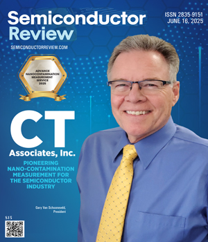
CT Associates, Inc. has been recognized by Semiconductor Review Magazine as “Advance Nanocontamination Measurement Service - 2025” based on our proprietary methodology, reflecting its position in the industry. This profile has been developed by the Semiconductor Review research and editorial team based on insights from an interview with Gary Van Schooneveld, President.



CT Associates, Inc.
Pioneering Nano-Contamination Measurement for the Semiconductor Industry
 Gary Van Schooneveld, President
At the heart of CT Associates’ mission is a commitment to detect, measure and control contamination in liquids, a challenging area that demands technical expertise, innovative problem-solving and new method development.
“Unlike conventional laboratory approaches that rely on extracting samples and analyzing them separately, we focus on a more dynamic route; measuring contamination in situ, directly within the operating equipment,” says Gary Van Schooneveld, President. “By doing so, we eliminate external contamination risks and achieve a level of accuracy that can improve detection by a factor of ten.”
This approach has made CT Associates a trusted partner in the semiconductor space, where contamination control is critical. Rather than offering one-size-fits-all testing, the company collaborates closely with its clients to understand their specific challenges and designs customized tests and equipment that yield actionable insights—not just a set of lab results, but data that drive real-world solutions.
Advancing Liquid Contamination Detection
As integrated circuits shrink and transistor densities increase, the presence of even a single particle can compromise an entire wafer. The traditional understanding of contamination revolved around particles visible under optical inspection tools. But as technology progressed, the need for more advanced measurement techniques became apparent. With device design rules identifying killer particle sizes well below 10 nanometers, contamination has become a critical challenge.
In the early days of contamination control, the industry was primarily focused on airborne particles as these were easier to detect, quantify and manage than in liquids. Cleanroom environments were designed to minimize particulate contamination, and air filtration systems were developed to ensure that semiconductor fabrication facilities maintained the highest standards of cleanliness.
Unlike conventional laboratory approaches that rely on extracting samples and analyzing them separately, we focus on a more dynamic route; measuring contamination in situ, directly within the operating equipment
As progress was made in managing airborne contamination, contamination in liquids, including ultrapure water and high-purity chemicals used in semiconductor processing, emerged as significant sources of contamination. Unlike airborne particles, which could be effectively controlled with filtration and airflow management, liquid-phase contaminants were far more challenging to detect and mitigate.
CT Associates pioneered methodologies focused on contamination measurement in liquids. This shift in focus proved revolutionary, providing semiconductor manufacturers with new insights into the sources of defects and yield loss.
CT Associates tackled this problem head-on by developing alternative measurement techniques that extended the detection capabilities into the 2-to-5 nanometer range. One of the most innovative approaches involved aerosol-based particle detection.
A breakthrough in this area was the ability to measure contamination in situ, meaning that samples did not have to be removed from the manufacturing environment for analysis. This eliminated the risk of external contamination and provided a much more accurate picture of the contamination levels within the production process.
Innovations in Nanoscale Liquid Contamination Measurement
As the industry continued to push the boundaries of miniaturization, it became clear that traditional contamination measurement methods were no longer sufficient. Optical particle counters, which had been the gold standard for measuring particles in liquids, struggled to detect particles below 30 nanometers. This posed a significant challenge, as semiconductor manufacturers were now working with device feature sizes in the single-digit nanometer range. If particles below the detection threshold were present in UPW and process chemicals, they could still cause defects, but manufacturers had no ability to measure them.
-
The SEMI C79 methodology provides a rigorous framework for evaluating filter performance, ensuring that semiconductor manufacturers can select the most effective filtration solutions for their processes
CT Associates tackled this problem head-on by developing alternative measurement techniques that extended the detection capabilities into the 2-to-5 nanometer range. One of the most innovative approaches involved aerosol-based particle detection.
By nebulizing liquid samples and converting them into an aerosol, the company could apply highly sensitive measurement technologies initially developed for airborne contamination. This breakthrough allowed for detecting particles as small as 1.8 nanometers, making it one of today’s most advanced contamination measurement techniques.
Establishing the Gold Standard in Semiconductor Cleanliness
Beyond particle detection, CT Associates also plays a pivotal role in developing industry standards for contamination control. One of the most significant contributions came with the development of SEMI C79, a standard for UPW filter performance testing. Liquid filtration systems are critical to semiconductor manufacturing, ensuring that process chemicals and ultrapure water remain contaminant-free.
“The SEMI C79 methodology provides a rigorous framework for evaluating filter performance, ensuring that semiconductor manufacturers can select the most effective filtration solutions for their processes,” says Van Schooneveld.
The development of SEMI C79 was not an isolated effort but the result of extensive collaboration with leading semiconductor manufacturers. One of the most notable partnerships was with Intel, which worked with CT Associates to validate the methodology through a multi-phase study.
A published collaborative study (Ryan Pavlick, Gary Van Schooneveld, Hokkin Choi, Vindhya Kunduru, David Neitling, Sriram Ramamoorthy, Vani Thirumala, “Evaluating Three Generations of UPW Filtration Technology Using SEMI C79”, Ultrapure Micro 2021) involved testing multiple generations of filters, applying the SEMI C79 methodology, and correlating the results with wafer-level defect analysis. The findings confirmed what many in the industry had long suspected—a direct relationship between nanoparticle retention performance and production wafer particle defect. This validation reinforced the importance of advanced filtration testing and established SEMI C79 as a global industry standard.
-7.jpg) nother significant contribution came with the development of SEMI C93, a standard for measuring contamination released by ion exchange resins. These resins play a crucial role in semiconductor manufacturing by purifying process chemicals and ultrapure water, removing metal ions and other impurities. They can also introduce contaminants of their own, particularly in the form of particle precursors. These dissolved contaminants may not initially appear as solid particles, but they can form under certain conditions, leading to wafer defects. The SEMI C93 methodology provided a standardized approach for evaluating resin quality, helping manufacturers select products that minimized contamination risks.
nother significant contribution came with the development of SEMI C93, a standard for measuring contamination released by ion exchange resins. These resins play a crucial role in semiconductor manufacturing by purifying process chemicals and ultrapure water, removing metal ions and other impurities. They can also introduce contaminants of their own, particularly in the form of particle precursors. These dissolved contaminants may not initially appear as solid particles, but they can form under certain conditions, leading to wafer defects. The SEMI C93 methodology provided a standardized approach for evaluating resin quality, helping manufacturers select products that minimized contamination risks.
Closing the Loop on Contamination Control
While detecting contamination in liquids is critical, the ultimate question for semiconductor manufacturers is whether these contaminants translate into wafer-level defects. Not all particles in a liquid system will transfer to a wafer surface, and understanding which ones do—and under what conditions—is essential for optimizing contamination control strategies. To address this challenge, CT Associates is working in collaboration with UNISERS AG, utilizing their Wafer Surface Inspection Tool, a state-of-the-art system for detecting, measuring and identifying nanoscale particles directly on wafer surfaces. It allows for a direct correlation between liquid-phase contamination and wafer-level defect formation, providing manufacturers with the data to more effectively refine their contamination control strategies.
CT Associates is also integrating advanced analytical techniques such as Fourier Transform Infrared (FTIR) spectroscopy and Surface-Enhanced Raman Spectroscopy (SERS) to provide chemical fingerprinting of contaminants. These methods go beyond simply counting particles. They allow manufacturers to understand what the particles are made of, providing crucial insights into contamination sources. By identifying the chemical composition of contaminants, manufacturers can take targeted actions to eliminate them from their processes, further improving yield and reliability.
-8.jpg) Collaboration has always been at the heart of CT Associates’ approach to innovation. The company works closely with semiconductor leaders, organizations and research institutions to drive advancements in contamination measurement. It actively contributes to and chairs/co-chairs International Roadmap for Devices and Systems (IRDS) and SEMI, committees, ensuring that its research aligns with the semiconductor industry’s evolving needs. Through ongoing partnerships, CT Associates continues to push the boundaries of what is possible in contamination detection and control.
Collaboration has always been at the heart of CT Associates’ approach to innovation. The company works closely with semiconductor leaders, organizations and research institutions to drive advancements in contamination measurement. It actively contributes to and chairs/co-chairs International Roadmap for Devices and Systems (IRDS) and SEMI, committees, ensuring that its research aligns with the semiconductor industry’s evolving needs. Through ongoing partnerships, CT Associates continues to push the boundaries of what is possible in contamination detection and control.
The continued focus on R & D and collaboration with established technical organizations and device manufacturers, has enabled CT Associates to publish over 150 technical papers over the past 3 decades earning them the reputation of being the center of excellence for contamination control. Besides technical papers, CT Associates has received 12 patents and been invited to present their technical results and lead sessions at the leading semiconductor conferences such as SPCC and Ultrafacility (formally Ultrapure Micro).
Reshaping Contamination Control at the Atomic Scale
Looking toward the future, CT Associates is exploring key research areas that have the potential to revolutionize contamination measurement. One area is advanced particle precursor detection, which focuses on identifying contaminants before they form defect-causing particles. This work includes expanding the scope of particle precursor detection to include IPA, a critical final rinse chemical. This proactive approach could enable manufacturers to prevent contamination-related defects before they occur.
As the semiconductor industry advances, the challenges associated with contamination control will only become more complex. CT Associates remains committed to its mission to be the global leader in nano-contamination measurement, providing semiconductor manufacturers with the most advanced tools and insights needed to achieve defect-free production. Through relentless innovation, strategic industry collaboration, and a commitment to excellence, the company is shaping the future of contamination control, ensuring that the next generation of semiconductor materials and devices meets the highest standards of purity and reliability.
With every breakthrough, CT Associates is not just measuring contamination—it is redefining the standards of cleanliness that drive the semiconductor industry forward.
| Share this Article:Tweet
|
Company
CT Associates, Inc.
Management
Gary Van Schooneveld, President
Description
CT Associates has been at the forefront of contamination measurement, evolving alongside the semiconductor industry’s ever-increasing demands for precision and purity. At the heart of CT Associates’ mission is a commitment to measuring and controlling contamination in liquids, a particularly challenging area that demands both technical expertise and innovative problem-solving.
This content is copyright protected
However, if you would like to share the information in this article, you may use the link below: