
Thank you for Subscribing to Semiconductor Review Weekly Brief
× 
Semi Conductor Review Weekly Brief
Be first to read the latest tech news, Industry Leader's Insights, and CIO interviews of medium and large enterprises exclusively from Semi Conductor Review
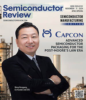
Capcon has been recognized by Semiconductor Review Magazine as “Top 10 Semiconductor Manufacturing Solutions Provider In Apac - 2024” based on our proprietary methodology, reflecting its position in the industry. This profile has been developed by the Semiconductor Review research and editorial team based on insights from an interview with Wang Honggang, Co-founder and CTO.



Capcon
Advanced Semiconductor Packaging for the Post-Moore’s Law Era

 Wang Honggang, Co-founder and CTO
Capcon cements its cornerstone here.
The young and dynamic engineering company helps the advanced semiconductor assembly and packaging industry push the boundaries of what’s possible with its equipment solutions, paving the way for the next generation of high-performance, compact devices with even lower cost.
Its competitive edge is in its core values of innovation, adaptability and customer-centricity, which enable it to overcome industry process challenges.
“We’re not interested in churning out cookiecutter solutions. Our goal is to co-create the future of semiconductor packaging with our clients, tackling the challenges that others shy away from,” says Wang Honggang, co-founder and CTO.
True to his words, Capcon’s focus on innovative solutions and customer collaboration helps clients maximize their production throughput or units per hour (UPH), covering both wafer-level and panel-level packaging.
This forward-thinking approach allows Capcon to address emerging needs in the rapidly evolving semiconductor industry, setting it apart from competitors.
The focus is not on standard processes. Instead, it concentrates on new processes and requirements that build upon standardized processes, which can bring the most value to end customers. The approach’s effectiveness is evident in the company’s market penetration. The solutions are already being used by top-tier semiconductor mass-manufacturers across Europe, Taiwan, Korea and China, including leading integrated device manufacturers (IDM).
Pioneering Advanced Packaging for AI and Beyond
Capcon’s approach to semiconductor packaging is evident in its versatile solutions, which span three key segments— bonding to substrate, wafer and panel. All are produced with precision and efficiency. Underpinned by patented technology, these solutions address the diverse and evolving needs of the industry.
All equipment features dual independent wafer stage and 12 placement heads at both front and rear, which allows simultaneous handling of various components within a compact footprint. This design maximizes efficiency while offering flexibility in feeding sources, accommodating wafers, tape reels, waffle pack trays and even JEDEC tray feeder.
“We’re proud to be the first company offering flexible, high-UPH solutions for panel-level packaging,” notes Honggang. “Our success is evident in our partnership with a leading European IDM, which now produces three million units daily using our machines, operating 24/7.”
A significant advantage of Capcon’s equipment is its ability to support both face-up and face-down bonding options for various packaging processes, in a single machine.
This versatility enables handling of multiple processes, including FOWLP, FOPLP, inFO, COW, SiP, CoWoS and eWLB, 2.5D, 3D —crucial in an industry where requirements change rapidly. 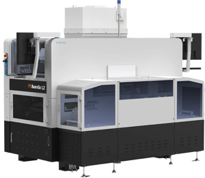 The latest A series and L series integrate these capabilities, reducing investment risk for customers. The A series caters to cutting-edge technologies like 2.5D, 3D and hybrid bonding, addressing the growing demands of AI chip production. Within this series, the A1 model specializes in hybrid bonding, while A2 and A6 cover 2.5D and 3D bonding, each tailored to different customer preferences in accuracy, flexibility and productivity.
Recognizing the high costs associated with AI chip fabrication, Capcon introduced the L series (Leo family) in 2023, focusing on panel-level solutions. This move addresses the industry’s shift toward more cost-effective alternatives to wafer-level packaging, a trend pursued by major players like Nvidia and AMD.
-
We’re not interested in churning out cookie-cutter solutions. Our goal is to co-create the future of semiconductor packaging with our clients, tackling the challenges that others shy away from
This adaptability is a game-changer for Capcon’s clients, enabling them to adjust production capabilities dynamically and accept orders from various design houses. The ability to change processes via software and recipes without investing in separate equipment offers significant cost savings and operational agility.
Capcon’s equipment typically delivers 50 percent higher or even double the UPH compared to competitors at the same cost, translating to a lower total cost of ownership—a critical factor in the competitive semiconductor industry.
A Multidisciplinary Approach
“Each team member contributes unique expertise to our shared vision, allowing us to tackle challenges together,” notes Honggang.
Capcon’s success in the semiconductor equipment industry stems from its diverse expertise and collaborative innovation. It unites specialists from mechanics, software, motion, optics and system control. This internal team is complemented by a network of external experts, including university fellows and retired professionals. This type of multidisciplinary approach is crucial in a field characterized by long development cycles and rapid technological advancements.
Encapsulated in its slogan, “connecting enabler,” Capcon works closely with customers to understand evolving needs and create customized, innovative solutions. Strategic partnerships with leading market players provide invaluable insights, ensuring development efforts align with current trends.
We’re proud to be the first company offering flexible, high-UPH solutions for panel-level packaging. Our success is evident in our partnership with a leading European IDM, who now produces three million units daily using our machines, operating 24/7
Rather than avoiding difficulties, Capcon embraces them as opportunities for growth. The company focuses on identifying promising directions aligned with industry trends, balancing diverse customer goals. This guides both strategic decisions and product development, positioning it to meet both current demands and future challenges.
Adapting to Change
“The issue isn’t change itself, but how we respond to it,” says Honggang, reflecting Capcon’s approach to staying competitive in a fast-paced industry.
Looking ahead, it plans to enhance its engineering capabilities to meet growing process requirements and design house requests. It will concentrate on advancing mass transfer technology and developing lower-cost interconnectivity technologies from a design perspective. Simultaneously, Capcon will address critical challenges in thermal efficiency applied packaging.
It is also pushing the envelope of accuracy in its products. By developing hybrid bonding technology, Capcon aims to deliver sub-micron precision for advanced computing requirements, demonstrating its commitment to higher accuracy.
In terms of long-term planning, a pragmatic approach is adopted. Rather than creating five- or 10-year plans that may become obsolete in the rapidly changing semiconductor industry, the company focuses on one-year cycles to remain agile and responsive to market shifts while maintaining a clear direction.
“If we can effectively plan for the next two years, we can win the battle,” says Honggang.
Capcon’s strategic positioning in the advanced semiconductor packaging space reflects a keen understanding of where the industry is headed. Its ability to transform complex challenges into high-performance solutions positions it well to capitalize on the industry’s shift toward advanced packaging techniques, potentially redefining the competitive landscape in the years to come.
| Share this Article:Tweet
|
Company
Capcon
Management
Wang Honggang, Co-founder and CTO
Description
Capcon, an equipment manufacturer in advanced semiconductor assembly and packaging, translates industry needs into innovative automation solutions. Its versatile machine-builder platform supports everything from wafer-level to panel-level packaging, optimizing high-value production environments.
This content is copyright protected
However, if you would like to share the information in this article, you may use the link below: