
Thank you for Subscribing to Semiconductor Review Weekly Brief
× 
Semi Conductor Review Weekly Brief
Be first to read the latest tech news, Industry Leader's Insights, and CIO interviews of medium and large enterprises exclusively from Semi Conductor Review
Adroit Materials has been recognized by Semiconductor Review Magazine as “Growth of III-Nitrides on ALN – Company of the Year - 2025” based on our proprietary methodology, reflecting its position in the industry. This profile has been developed by the Semiconductor Review research and editorial team based on insights from an interview with Dr. Kirste, COO.



Adroit Materials
Redefining Epitaxy with Boutique Precision

 Dr. Kirste, COO
What sets Adroit Materials apart is its proprietary technology and deep expertise in growing ultra-high-quality III-nitride device structures directly on single-crystalline aluminum nitride (AlN) or gallium nitride (GaN) substrates. This approach delivers a million-fold improvement in crystal quality compared to conventional methods using sapphire, silicon, or silicon carbide substrates—translating to dramatically enhanced device performance, reliability, and thermal management.
Adroit Materials is purpose-built to support researchers, startups, and development teams creating devices that don’t fit within traditional semiconductor manufacturing workflows. Rather than focusing on high-volume production, the company has adopted a boutique approach to epitaxy, delivering device layers with unmatched precision. Unlike large foundries geared for scale, Adroit Materials is agile—designed for rapid prototyping, customized material solutions, and accelerated experimental iteration, all without sacrificing crystal quality.
“We’re not trying to be the TSMC of wide bandgap materials,” says Dr. Kirste, COO of Adroit Materials. “We aim to be the go-to partner for innovation—where researchers and engineers can realize their ideas quickly and without compromise.”
A Collaborative, Boutique Foundry Model
Adroit Materials’ business model is tailored for early-stage innovation. Its customers typically require low-volume prototypes—often just a handful of wafers—of novel, non-standard device structures with tight quality control and fast feedback loops. These needs are rarely met by large-scale foundries, where even a minor process change can trigger months of revalidation. In contrast, Adroit Materials offers hands-on engagement and process flexibility, acting more like an extension of its clients’ R&D teams than a traditional vendor.
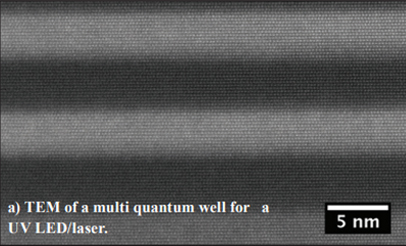 This collaborative model is a key differentiator. Instead of supplying off-the-shelf wafers, Adroit Materials co-develops material stacks with customers—tuning doping levels, layer compositions, and film thicknesses based on evolving performance goals. The result: a significantly faster design–build–test cycle, enabling customers to accelerate innovation while collecting high-confidence data from production-grade materials.
Crucially, Adroit Materials adapts to each project’s specific needs. This agility is vital for customers exploring the limits of material science. For those who need it, we also offer downstream fabrication support—allowing clients to move seamlessly from epitaxy to full-stack device prototyping within a unified workflow.
Aluminum Nitride: A Challenging but Strategic Material
These materials are particularly relevant for next-generation defense systems, including high-frequency radar, directed energy weapons, and radiation-tolerant space electronics. However, their growth and property control are notoriously difficult—an area where Adroit Materials stands among the few capable players.
Adroit Materials has built deep technical expertise in two of the most demanding yet promising wide bandgap semiconductors: AlN and AlGaN. Aluminum nitride, with its wide bandgap (6.1 eV), high thermal conductivity, exceptional thermal stability, and radiation hardness, is a strategic material for applications ranging from UV-C LEDs and high electron mobility transistors (HEMTs) to power electronics and quantum photonics.
-
We aim to be the go-to partner for innovation—where researchers and engineers can realize their ideas quickly and without compromise.
These materials are particularly relevant for next-generation defense systems, including high-frequency radar, directed energy weapons, and radiation-tolerant space electronics. However, their growth and property control are notoriously difficult—an area where Adroit Materials stands among the few capable players.
In close collaboration with the Department of Materials Science and Engineering at North Carolina State University, Adroit Materials has refined its AlN and AlGaN growth processes using metal-organic chemical vapor deposition (MOCVD). The process incorporates internal and external controls, in situ metrology, and advanced process modeling—enabling the production of films with exceptional uniformity, surface quality, and purity.
As a result, customers have reported measurable improvements in yield, thermal performance, and long-term reliability when using Adroit Materials’ epitaxial wafers.
Filling a Critical Gap in the Semiconductor Ecosystem
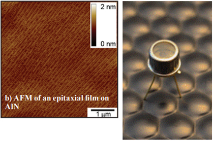 A key gap in the semiconductor value chain lies between fundamental materials science and commercial fabrication. University labs and startups often create promising device concepts but lack the infrastructure to produce the high-quality epitaxial materials required for proof-of-concept testing. At the same time, large foundries are rarely equipped—or incentivized—to handle low-volume, high-risk, iterative development.
Adroit Materials fills this gap by operating as a boutique foundry for innovation. Its customer base includes national laboratories developing quantum devices, defense contractors requiring radiation-hard materials, startups building UV-C disinfection LEDs, and OEMs prototyping wide bandgap power devices. In every case, Adroit Materials’ ability to deliver custom materials and structures with speed and precision bridges the divide between research and scalable manufacturing.
Next to crystal quality, turnaround time is one of Adroit Materials’ most valued attributes. While traditional foundries might require six months to deliver a new wafer design, Adroit Materials often delivers in just a few weeks. This responsiveness, combined with technical expertise, provides a significant advantage for teams iterating on early-stage designs or preparing for commercialization.
For instance, a quantum device startup approached Adroit Materials after months of delays and inconsistent wafer quality from another foundry. Within weeks, we leveraged in situ metrology and adaptive modeling to optimize the layer structures and doping levels, delivering production-grade wafers with exceptional uniformity and low defect density— cutting lead time by over 75% and helping the customer meet critical investor milestones.
Looking Ahead: Growth Without Compromise
Although Adroit Materials maintains a boutique mindset, it is expanding its toolsets and metrology capabilities to meet growing demand. Rather than pursuing commodity-scale contracts, the company is doubling down on its role as a strategic innovation partner.
Future plans include:
• Expansion into InGaN foundry services
• Development of vertical GaN devices on native GaN substrates
• Adoption of novel growth techniques such as HVPE
• Ongoing refinement of AlN and AlGaN processes to unlock even higher electronic performance
As the semiconductor industry evolves to meet the demands of electrification, advanced communications, and quantum technologies, the need for high-performance materials will only intensify. Adroit Materials isn’t trying to be everything to everyone—but for those working at the edge of what’s possible, it just might be exactly the partner they need.
| Share this Article:Tweet
|
Company
Adroit Materials
Management
Dr. Kirste, COO and Dr. Zlatko Sitar, CEO
Description
Adroit Materials specializes in III-nitride semiconductor technology. The company offers advanced epitaxial growth, doping and strain management services to enhance electronic and optoelectronic device performance. The company’s product line includes high-power ultraviolet light sources, Al rich AlGaN HEMTs, and GaN vertical power diodes and solar-blind avalanche photodiodes, catering to applications in disinfection, space exploration, and defense.
This content is copyright protected
However, if you would like to share the information in this article, you may use the link below: